


 2025-12-10
 BEST
BEST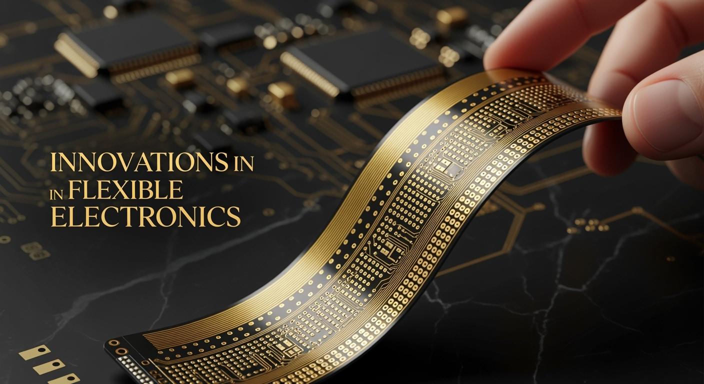
You see high-density FPC (HDI FPCB) as an important technology. It helps make electronics smaller and easier to carry. This flexible circuit lets you reach hard design goals. Devices can be smaller, lighter, and faster. The world market for these boards was over $23 billion in 2024. It might more than double by 2030. If you work in engineering or manufacturing, this fast growth is important. Knowing about it helps you stay ahead of others.
Key Takeaways
- High-density FPC (HDI FPCB) technology helps make devices smaller and lighter. It also makes them faster. This is very important for new engineering today.
- Microvias and many layers in HDI FPCBs help fit complex designs in small spaces. This makes signals better and helps the device work well.
- It is very important to control crosstalk and impedance in HDI FPC design. Good spacing and the right trace width can make signals much better.
- Laser drilling is a main way to make HDI FPCBs. It makes holes the right size and cuts down on waste when making them.
- Using HDI FPCBs can save money and make devices work better. They are used in things like electronics for people and medical tools.
What Is High-Density FPC (HDI FPCB)?
Core Features and Structure
You find high-density FPC (HDI FPCB) in new electronics. This technology uses microvias. Microvias are very small holes that link layers together. These holes are smaller than 0.15mm wide. Makers use lasers or chemicals to make them. You see these in devices that need small and strong connections.
High-density FPC (HDI FPCB) is special because it can have more layers than normal boards. Some designs have 4 to 20 layers. The lines and spaces can be as tiny as 40μm. This lets you fit more circuits in less space. This setup makes signals better and helps make products smaller.
Here is a table with the main technical details:
| Specification | HDI (High-Density Interconnect) |
|---|---|
| Microvias | Yes, includes stacked or staggered microvias |
| Layer Count | Typically 4 to 20 layers |
| Line Width/Spacing | 40μm/40μm (1.6mil/1.6mil) or smaller |
| Key Features | Enhances signal integrity and miniaturization |
| Common Applications | Smartphone motherboards, automotive electronics, AI hardware |
These features help when you need high-density flexible printed circuit boards for tough jobs. The tiny microvias and thin lines let you make circuits that fit in small places. This makes it easier to try new ideas in your work.
You can also check the sizes of microvias and how close the circuits are:
| Parameter | Value |
|---|---|
| Finer lines and spaces | ≤ 100 µm (0.10mm) |
| Microvias diameter | < 150 µm |
| Capture pads | < 400 µm |
| Pad density | > 20 pads/cm² |
These numbers show how high-density FPC (HDI FPCB) lets you build small and complex designs.
Comparison with Standard Flexible Circuit Board
You can see big differences between high-density FPC (HDI FPCB) and a normal flexible circuit board. The biggest difference is the number of layers and the size of the parts. High-density FPC (HDI FPCB) can have more layers and thinner materials. Normal flexible circuit boards have 4 to 12 layers, but they are not as dense.
Here is a table to compare:
| Type of PCB | Layer Count |
|---|---|
| HDI PCB | Higher layer counts with thinner substrates |
| Standard Multilayer PCB | Typically 4 to 12 layers |
High-density FPC (HDI FPCB) also uses special microvia technology. This lets you make thinner lines and smaller spaces between them. Normal flexible circuit boards cannot do this. If you need a design that is small and works well, you pick high-density FPC (HDI FPCB).
Tip: If your project needs lots of connections in a tiny space, high-density FPC (HDI FPCB) is the best choice. You get good performance and a smaller device.
You use high-density FPC (HDI FPCB) when you want to do more with flexible printed circuit boards. This helps you meet the hard needs of today’s electronics.
Managing Crosstalk and Impedance in FPCB
When you use high-density FPC, you face new problems with signals. Crosstalk and impedance control are very important. As you make devices smaller, these issues get harder. You need to know how to handle them from the start if you want your design to work well.
Trace Width and Spacing for High-Density FPC
Crosstalk happens when signals in one trace mess with another. In high-density FPC, this is common because traces and vias are close together. The main causes of crosstalk are:
- Track-to-track and via-to-track coupling, which makes unwanted noise.
- Ground bounce, where shared return paths for fast signals cause noise.
- Power supply crosstalk, where big current changes affect nearby traces.
To lower crosstalk, you must watch trace width and spacing. The table below shows how much space to leave for each signal type:
| Signal Type | Recommended Spacing |
|---|---|
| High-Frequency Signals | More than 4 times the trace width (depends on frequency) |
| Sensitive Components | 2 to 3 times the trace width (depends on sensitivity) |
Keep high-frequency traces far apart. This stops unwanted connections and keeps signals clean. For sensitive parts, leave enough space to keep out noise.
Impedance control is also very important in high-density FPC. If you do not control impedance, signals can bounce back and get lost. Here are ways to keep impedance steady:
- Place fast signal layers between solid ground planes.
- Control trace width and spacing, keeping at least three times the trace width between traces.
- Use microvias in the right spots, and cut down via stubs with special drilling.
- Add ground planes and put decoupling capacitors near the signal source.
- Use differential signaling to lower crosstalk and noise in fast data lines.
- Pick materials like Rogers 4350B for better high-frequency work.
The material you pick also changes impedance. The dielectric constant (Dk) of your material sets the impedance of your lines. If you choose the right Dk and dissipation factor (Df), you keep impedance steady. If the material changes, impedance can change too, which causes signal trouble.
Tip: Always check the Dk and Df of your materials before you start. This helps you avoid mistakes that cost money later.
Microvias and new via technology help you make more connections in less space. You can use stacked microvias, via-in-pad, and laser drilling to fit more in. These ways help make things smaller and make assembly faster. The table below shows common via types:
| Technology Type | Description |
|---|---|
| Microvias | Small vias that connect HDI substrates and PCB layers, saving space. |
| Blind and Buried Vias | Vias that do not go through the whole board, so you can have more layers and better circuits. |
| Laser Drilling | A careful way to make small vias, needed for high-density jobs. |
When you use these new via types, you can fit more wires without losing strength. Microvias help you keep up with new packaging and make electronics smaller.
You also need to think about reliability with microvias. Staggered microvias spread out stress and make things stronger when they heat up and cool down. Stacked microvias save space but need careful control of fill and grain. If you do not manage these things, you might see problems like cracks or gaps.
Advanced Manufacturing for High-Density FPC
Laser Drilling Vias in High-Density FPC Manufacturing
When making high-density flex pcb, you need special ways to build it. Laser drilling is the most common way to make microvias in flex pcb. This uses a strong laser beam to burn away material and make tiny, exact holes. You can make holes as small as 0.075mm. This is great for connecting small parts in your flex pcb.
Laser drilling gives many good things for flex pcb:
- You get very exact hole sizes, sometimes as small as 30 μm.
- The holes can be deep compared to their width, up to 15:1.
- The laser puts holes in the right spot, within ±15 μm.
- The laser does not hurt the dielectric material much.
- The process is clean, with no waste liquid or drill bits.
Note: Laser drilling can make vias with a tolerance of ±10 μm in flex pcb. This accuracy is very important for good electrical work, especially in hard designs.
Here is a table that shows common ways to make HDI flex pcb:
| Process Type | Description |
|---|---|
| Via Metallization | Filling and covering vias so they are solid and connect well. |
| Laser Drilling | Using a strong beam to remove material and make microvia holes. |
| Chemical Etching | Fast way to make small vias, up to 12,000 each second. |
| Plasma/Photovia Formation | Other ways to make small vias quickly. |
You can use these ways to make flex pcb with 2 to 30 layers. Factories can make up to 3000m² each day, so they can fill big orders.
Laser drilling also lets you put more circuits in a small space on flex pcb. This is important for new electronics. Picking the right laser settings and drilling plans is very important. If you control these, you get the same good results every time in your flex pcb.
You should know that laser-drilled vias have tighter hole location limits than mechanical drilling. This helps you keep holes lined up, so your flex pcb works right.
Tip: Always check if your flex pcb maker can do laser drilling well. Good tolerances and accuracy help you get the best design.
Reliability and Cost Considerations
Rigid-Flex PCB vs High-Density FPC Cost Analysis
When you look at rigid-flex PCBs and high-density flexible circuit boards, you see different things that change the price. Flexible PCB materials like polyimide cost more than FR4 in rigid boards. Making flexible circuit boards takes more steps and is harder, especially for multilayer and rigid-flex types. This makes the price go up.
The number of layers, the kind of material, and the shape of your design all change the final cost. If you add more layers to flexible circuit boards, it costs more and is harder to make. Flexible materials can break more easily, so fewer good boards are made, which also raises the price.
Here is a table that shows the usual cost for each high-density flexible circuit board at different amounts:
| Production Volume | HDI FPCBs Cost Range | Rigid-Flex PCBs Cost Range |
|---|---|---|
| Prototypes (5–10 pcs) | $12–$45 per piece | N/A |
| Mid-volume (100–500 pcs) | $4–$15 per piece | N/A |
| Mass production (1000+ pcs) | $0.80–$3 per piece | N/A |
| Higher complexity (HDI) | Generally more expensive than rigid-flex | N/A |
Rigid-flex PCBs often cost more at the start because they are harder to make. Sometimes, you save money later, but high-density flexible circuit boards usually cost more if the design is very complex.
Tip: You can save money by making your design better and picking the best materials for your flexible printed circuit assembly.
Reliability Testing of High-Density Flexible Circuits
You need to make sure flexible circuit boards work well, especially in tough jobs. There are many rules and tests to check reliability, like IPC-2221 Appendix A, Conductor Analysis Technology (CAT), Printed Circuit Quality and Relative Reliability (PCQR2), Highly Accelerated Thermal Shock (HATS), and Interconnect Stress Test (IST). These tests help you know if your flexible circuit boards will work in real life.
The most common problems you might see are:
- Microvia voids, which make weak spots and can stop signals.
- Layer misalignment, which breaks connections in tight circuits.
- Delamination, which lets water in and can cause heat problems.
You need to fix these risks early in your design to make sure your boards are strong. Careful steps in making and lots of testing help you stop these problems. Flexible circuit boards are used in important things like medical devices and car electronics, where they must work well.
Note: Always ask your supplier for full reliability test results before you start making a lot of boards.
You get lots of good things when you pick HDI FPCBs for your design.
- They cost less and take up less space.
- You have more ways to design your project.
- They work better with electricity and heat.
- The connections are strong, and you can put them together faster.
HDI FPCBs help make new ideas in wearables, phones, and medical tools. They are used in many different things, as shown below:
| Application Area | Examples |
|---|---|
| Consumer Electronics | Mobile phones, tablets, laptops |
| Automotive Industry | ADAS, infotainment systems |
| Medical Devices | Pacemakers, diagnostic tools |
| Aerospace and Defense | Satellites, military equipment |
By using HDI FPCBs, you can help shape the future of electronics.
FAQ
What is a flexible circuit?
A flexible circuit connects parts in things that can bend. It fits into small and tight spaces. This helps make products lighter and thinner. You see flexible circuits in phones, cameras, and medical devices.
Why should you choose a flexible circuit for your project?
You pick a flexible circuit if you want something light and thin. It bends easily and fits in small places. This type of circuit lowers weight and makes things work better. Many companies use flexible circuits for new products.
How does a flexible circuit improve signal quality?
Flexible circuits help signals stay clear and strong. They cut down on noise and crosstalk. Short paths let signals move faster. This means fewer mistakes in fast designs.
What are the main steps in flexible circuit design?
First, you plan how the circuit will look. Next, you pick the right materials. You check the size and shape to fit your needs. Then, you test the circuit for strength and how well it works. Good planning stops problems later.
Where do you see flexible circuit technology used most?
Flexible circuits are in smartphones and wearables. Medical devices use them too. Cars and airplanes also need flexible circuits. These places need circuits that bend and last long.
.png)
.png)
.png)
.png)

.png)

