


 2025-09-04
 BEST
BEST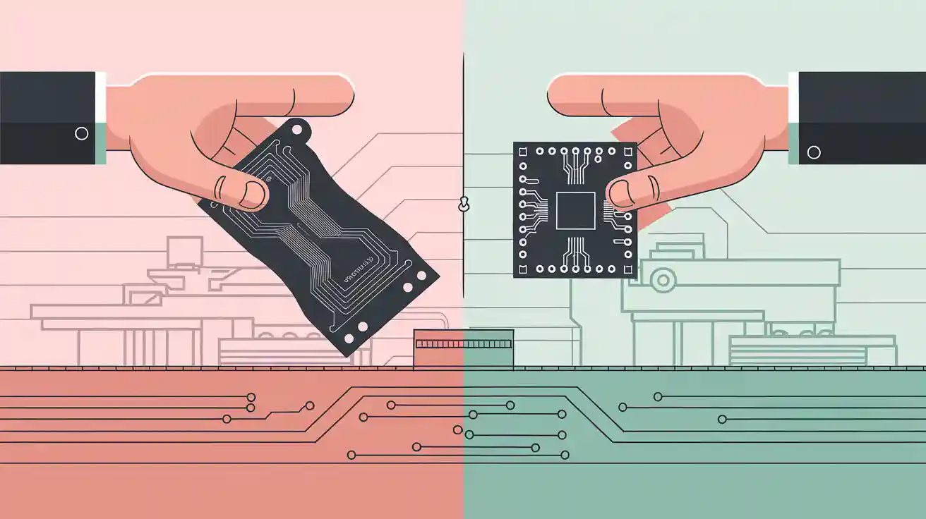
When you compare additive flex pcb manufacturing to traditional approaches, you see clear differences in efficiency, waste, and design freedom. Additive processes allow you to create flexible printed circuit boards with high customization and less material waste. You gain faster production cycles and more adaptable solutions for complex applications. The table below highlights how additive and traditional methods stack up in key areas:
| Aspect | Additive Manufacturing | Traditional Manufacturing |
|---|---|---|
| Customization | High | Limited |
| Waste Reduction | Significant | High |
| Efficiency | Improved | Slower |
| Flexibility | High | Low |
| Potential Applications | 3D printing in space missions | Standard electronic devices |
Key Takeaways
- Additive flex PCB manufacturing offers high customization and reduces material waste, making it ideal for complex designs and rapid prototyping.
- Traditional PCB methods are best for high-volume production, providing reliability and lower costs per unit for standardized designs.
- Choosing the right manufacturing method depends on your project's design requirements, budget, and production volume.
- Additive processes allow for faster production cycles, enabling quicker iterations and responses to customer needs.
- Consider a hybrid approach: use additive methods for prototyping and traditional methods for mass production to optimize speed and cost.
PCB Manufacturing Methods
When you explore pcb manufacturing methods, you encounter a range of options that suit different design needs and production goals. You can choose between additive flex PCB processes and traditional techniques, each offering unique advantages for electronics manufacturing.
Additive Flex PCB Overview
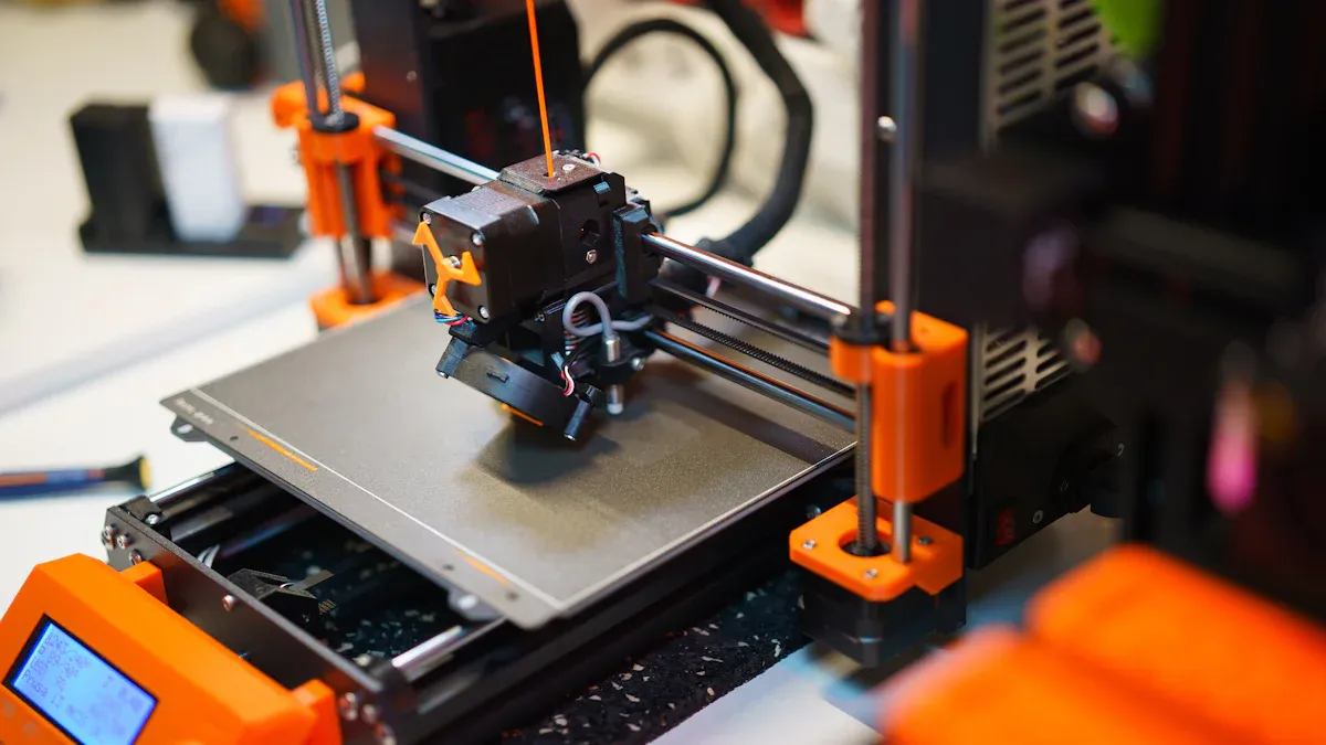
Additive flex PCB manufacturing stands out among pcb manufacturing methods for its innovative approach. You build circuit paths layer by layer using conductive inks and flexible substrates. This method uses specialized PCB printers that deliver high precision. You gain the ability to create intricate designs and adapt to complex shapes. Additive flex PCB processes minimize waste because you only deposit material where needed. You also benefit from faster prototyping cycles, which help you iterate designs quickly. Many engineers in Nigeria prefer this method for custom electronics and rapid development.
- Additive manufacturing builds circuit paths layer by layer.
- You use conductive inks and flexible substrates.
- Specialized printers enable high-precision results.
- Waste reduction is significant compared to other pcb manufacturing methods.
| Aspect | Additive Flex PCB Process |
|---|---|
| Workflow | Utilizes conductive inks and specific substrates |
| Equipment | Requires specialized PCB printers for high precision |
| Design Software | Varies significantly in precision and capabilities |
Traditional Methods Overview
Traditional pcb manufacturing methods rely on subtractive techniques. You start with a solid substrate and remove unwanted material to form circuit paths. This process often uses chemicals and etching solutions. You can select from several types of PCBs, including single-sided, double-sided, multi-layered, rigid, and flex PCBs. These methods require a wider range of equipment and standardized design software. You may find traditional methods more suitable for high-volume production and standard electronic devices.
- Traditional methods often involve removing material to create desired shapes.
- You use chemicals and etching solutions.
- Standardized design software supports these pcb manufacturing methods.
- Equipment includes a variety of tools for material handling and processing.
Here are the main types of pcb manufacturing methods you will encounter:
- Single-Sided PCBs: Components on one side, conductive paths on the other.
- Double-Sided PCBs: Conductive material on both sides for more complex designs.
- Multi-layered PCBs: Three or more layers, ideal for high-speed circuits.
- Rigid PCBs: Solid substrate for strength and stability.
- Flex PCBs: Flexible designs for dense signal connections.
Tip: When choosing between pcb manufacturing methods, consider your design complexity, production volume, and required flexibility. Additive flex PCB processes excel in customization and waste reduction, while traditional methods offer reliability for standard applications.
Additive Manufacturing Process
Steps in Additive Flex PCB
You follow a precise sequence when you use additive manufacturing technology for flex PCB production. The additive process builds up the circuit layer by layer, which gives you more control over the final product. Here are the main steps you will encounter in the additive process:
- Start with a dielectric core and apply a tie layer to prepare the surface.
- Apply and expose photoresist to define the circuit pattern.
- Electroplate copper onto the desired features, forming the conductive traces.
- Strip the resist to reveal the plated areas.
- Etch away the unplated seed layer, leaving only the intended copper traces.
- Complete the final finish and via plating to ensure electrical connectivity.
This additive process uses advanced additive manufacturing technology at each stage. You can achieve high precision and repeatability, which is essential for modern electronics.
Additive Manufacturing Technology
Additive manufacturing technology transforms how you approach flex PCB design and production. When you use additive manufacturing, you deposit materials only where needed. This method stands in contrast to traditional subtractive techniques, which often waste valuable resources. Additive manufacturing technology, such as screen printing with conductive inks, allows you to create complex circuit paths without unnecessary material loss. You gain the ability to design intricate layouts and adapt to unique shapes, which is especially useful for custom or low-volume projects.
Additive manufacturing technology also supports rapid prototyping. You can quickly test new ideas and make changes without waiting for long production cycles. The flexibility of additive manufacturing technology means you can respond to customer needs faster and reduce time to market. You also benefit from a cleaner process, as additive manufacturing technology minimizes chemical use and environmental impact.
Note: Additive manufacturing technology gives you a competitive edge by reducing waste, improving design freedom, and supporting sustainable production. If you want to stay ahead in the electronics industry, you should consider integrating additive manufacturing technology into your workflow.
Traditional Process Steps
Subtractive Workflow
You encounter a detailed workflow when you use traditional manufacturing for flex PCBs. Subtractive methods dominate this process. You start with a copper-clad laminate and remove unwanted copper to create circuit patterns. Subtractive techniques define the core of traditional manufacturing. You rely on subtractive processes to achieve precise traces and pads. The workflow for traditional manufacturing includes several steps, each critical for quality and consistency.
Here is a typical sequence you follow in traditional manufacturing:
| Step Number | Step Description |
|---|---|
| 1 | Inner Layer Imaging |
| 2 | Inner Layer Etching |
| 3 | Resist Stripping |
| 4 | Inner Layer AOI |
| 5 | Inner Layer Oxide |
| 6 | Layup |
| 7 | Lamination |
| 8 | X-Ray Alignment |
| 9 | Drilling |
| 10 | PCB Plating |
| 11 | Outer Layer Imaging |
| 12 | Outer Layer Etching |
| 13 | Outer Layer AOI |
| 14 | Solder Mask Application |
| 15 | Silkscreen Application and Surface Finish Application |
| 16 | Finishing the PCB |
You see that traditional manufacturing technology uses subtractive steps at multiple stages. You image and etch both inner and outer layers. You strip resist and apply oxide. You laminate layers and align them with X-ray. You drill holes and plate them. You finish with solder mask, silkscreen, and surface treatments. Subtractive actions repeat throughout traditional manufacturing, ensuring the final PCB meets design requirements.
Tip: You can optimize your workflow by monitoring each subtractive step. Careful control of imaging, etching, and plating improves yield and reduces defects in traditional manufacturing.
Material and Chemical Use
Traditional manufacturing relies on a wide range of materials and chemicals. Subtractive processes use copper, resists, and etchants. You also encounter hazardous substances in traditional manufacturing. These include lead, brominated flame retardants, cadmium, mercury, hexavalent chromium, nickel, and perfluorinated compounds. Each material plays a role in subtractive steps, but many pose environmental and health risks.
| Material/Chemical | Environmental Impact |
|---|---|
| Lead (Pb) | Toxic exposure leading to neurological issues, especially in children. |
| Brominated Flame Retardants (BFRs) | Persistent pollutants causing endocrine disruption and bioaccumulation in wildlife. |
| Cadmium (Cd) | Carcinogenic effects, kidney damage, and respiratory problems. |
| Mercury (Hg) | Highly toxic, impairing neurological functions. |
| Hexavalent Chromium (Cr6+) | Potent carcinogen, regulated due to environmental concerns. |
| Nickel (Ni) | Allergic reactions and respiratory issues from prolonged exposure. |
| Perfluorinated Compounds (PFCs) | Persistent in the environment, posing potential health risks. |
You must handle these chemicals with care during traditional manufacturing. Subtractive methods generate waste that requires proper disposal. You see strict regulations for many substances used in traditional manufacturing technology. You protect workers and the environment by following best practices for chemical handling and waste management. Subtractive techniques remain effective, but you must balance performance with safety and sustainability.
Additive Flex PCB vs Traditional: Key Differences
Cost Comparison
When you evaluate the cost of manufacturing printed circuit boards, you notice significant differences between additive flex pcb and traditional methods. Additive flex pcb processes often require specialized equipment and materials, which can increase the initial cost. However, you benefit from reduced setup and tooling expenses, especially for small production runs or prototypes. Traditional methods, on the other hand, may offer lower cost per unit for high-volume production due to established workflows and economies of scale.
Here is a table that compares the average cost per square inch for different types of printed circuit boards:
| Type of PCB | Cost per square inch | Cost Comparison |
|---|---|---|
| Flexible PCBs | $0.50 to $15.00 | 2-5x premium over rigid |
| Rigid-flex PCBs | $1.00 to $25.00 | Higher due to complexity |
You should consider the total cost, including waste management and environmental compliance. Additive flex pcb manufacturing reduces waste, which can lower your overall cost in the long run. If you need frequent design changes or custom shapes, additive flex pcb offers a cost advantage by eliminating the need for new tooling. For mass production of standard printed circuit boards, traditional methods may still provide the lowest cost per unit.
Tip: If your project involves low to medium volumes, frequent design changes, or complex geometries, additive flex pcb can help you control cost and reduce waste.
Production Speed
Production speed plays a crucial role when you select a manufacturing method for printed circuit boards. Additive flex pcb processes streamline production by building circuits layer by layer, which allows you to move from design to finished product quickly. You can produce prototypes in hours instead of days, enabling rapid iteration and faster time to market.
Traditional manufacturing of printed circuit boards involves multiple steps, such as imaging, etching, drilling, and plating. Each step adds time and complexity, especially for multi-layer or rigid-flex designs. You may face delays due to tooling changes or setup requirements. Additive flex pcb methods eliminate many of these steps, so you can respond to customer needs faster and reduce lead times.
If you value speed and flexibility, additive flex pcb gives you a clear advantage. For large-scale production of standard printed circuit boards, traditional methods may still deliver consistent throughput, but you sacrifice agility.
Material Waste
Material waste remains a major concern in printed circuit boards manufacturing. Traditional methods rely on subtractive processes, where you start with a copper-clad substrate and remove excess material through etching. This approach generates significant waste, including hazardous chemicals and scrap copper. You must manage and dispose of this waste, which increases your cost and environmental impact.
Additive flex pcb manufacturing addresses this challenge by depositing materials only where needed. You build the circuit layer by layer, using conductive inks and flexible substrates. This process reduces material waste by as much as 50% compared to traditional methods. You also avoid the use of toxic chemicals, making additive flex pcb a more sustainable choice.
- Additive flex pcb processes use biodegradable materials like cellulose-based films and PLA, which decompose naturally and reduce e-waste.
- You eliminate the need for fasteners and extra assembly steps, further minimizing waste.
- The layer-by-layer approach aligns with circular manufacturing principles, lowering your environmental footprint.
If you want to meet sustainability goals and reduce your cost of waste management, additive flex pcb offers a clear benefit over traditional printed circuit boards manufacturing.
Surface Quality
Surface quality affects the performance and reliability of printed circuit boards, especially in high-frequency or sensitive applications. Traditional manufacturing methods have established standards for surface finish, which ensures consistent quality across large batches. You can achieve smooth, uniform surfaces that support reliable soldering and signal integrity.
Additive flex pcb manufacturing faces unique challenges in this area. The use of a single material can limit your design options and affect performance. Achieving a suitable surface finish requires careful control of the printing process. Rough surfaces can impact the performance of high-frequency circuits, leading to signal loss or interference. Quality control remains a challenge, as the industry lacks standardized testing and certification for additive flex pcb.
- You must select materials carefully to balance flexibility and surface quality.
- Surface finish remains critical for high-speed or RF printed circuit boards.
- The lack of established standards can complicate testing and certification, affecting reliability.
Note: If your application demands the highest surface quality and proven reliability, traditional printed circuit boards may be the better choice. For rapid prototyping or custom designs, additive flex pcb provides flexibility, but you should monitor surface finish closely.
Design Flexibility and 3D Printed PCBs
Complex Geometries
You gain a significant advantage with 3d printed pcbs when you need to create complex shapes and non-planar designs. Additive manufacturing lets you print circuits on curved surfaces, vary thicknesses, and even embed components on the sides of a substrate. You can design interconnect vias in horizontal, diagonal, or curved orientations, which traditional PCB processes cannot easily achieve.
- You print circuits on flexible, curved, or irregular surfaces.
- You embed or mount components on non-planar areas.
- You create unique interconnects that follow any path you design.
Unlike traditional PCB manufacturing, which limits you to flat, layered boards, 3d printed pcbs remove these restrictions. You realize your ideas without compromising on geometry or layout. This level of flexibility and customization supports advanced applications, such as wearables, IoT devices, and aerospace electronics.
| Limitation (Traditional PCBs) | Description |
|---|---|
| Manufacturing Complexity | Non-standard shapes require specialized tooling, raising costs and production time. |
| Component Placement and Routing | Irregular shapes limit component space and complicate trace layout. |
| Mechanical Stress and Durability | Non-rectangular designs face higher risk of cracks and stress failures. |
Customization and Iteration
3d printed pcbs give you unmatched control over customization and rapid design iterations. You can prototype new designs in-house, test them quickly, and make changes without waiting for external suppliers. This process saves you time and money, especially for small batches or custom projects.
| Advantage | Description |
|---|---|
| Rapid Prototyping | You create and test PCB designs quickly. |
| Design Flexibility | You modify and iterate designs with ease. |
| Cost-Effective for Small Batches | You save money on small runs or custom layouts. |
You benefit from 3d printed pcbs by producing prototypes much faster than with traditional methods. This speed is crucial during research and development, where you often need to refine your product through multiple quick iterations. You can tweak your design, print a new version, and test it—all in a single day.
- 3d printed pcbs enable you to prototype and improve designs in-house.
- You achieve mass customization for unique applications.
- You respond to customer needs with rapid design iterations.
Note: 3d printed pcbs empower you to deliver innovative solutions, reduce waste, and accelerate your product development cycle. You stay ahead in the market by leveraging their flexibility and customization.
Application Suitability
Best Uses for Additive Flex PCB
You should choose the additive flex PCB method when you need high customization, complex shapes, or rapid prototyping. This method works best for projects that require quick design changes or small production runs. You can use this method to create flexible circuits for advanced applications. Many engineers rely on this method for rapid prototyping because it reduces lead time and material waste.
Here is a table showing where the additive flex PCB method excels:
| Application Type | Industry |
|---|---|
| High-Density Interconnects (HDIs) | Consumer Electronics |
| Flexible and Rigid-Flex PCBs | Medical Devices |
| Advanced Driver Assistance Systems | Automotive |
| Implantable Sensors | Medical Devices |
| Wearable Health Monitors | Medical Devices |
| Infotainment Systems | Automotive |
| Electric Vehicle Components | Automotive |
| Testing Equipment | Various Industries |
| Tools | Various Industries |
| Compact Electronics | Consumer Electronics |
You can also use this method for prototyping in industries like automotive, healthcare, and consumer electronics. The method supports rapid prototyping for wearable health monitors, implantable sensors, and electric vehicle components. You gain the ability to test and refine your designs quickly, which is essential for innovation.
Tip: If you need to create unique layouts or test new ideas, the additive flex PCB method gives you the flexibility and speed you need.
Best Uses for Traditional Methods
You should select traditional methods when you need high-volume production, proven reliability, or standardized designs. This method remains the industry standard for mass manufacturing. You can use these methods for consumer electronics, automotive systems, and industrial equipment. Traditional methods support prototyping for large batches and deliver consistent quality.
You will find traditional methods most effective in these areas:
- Consumer electronics such as smartphones, laptops, and TVs
- Automotive electronics for modern vehicles
- Medical devices like pacemakers and ventilators
- Industrial automation systems and control panels
- Aerospace and telecommunications equipment
This method offers cost advantages for large-scale projects. You benefit from established workflows and quality standards. When you need to produce thousands of units with minimal variation, traditional methods provide the best results.
Note: For projects that demand high reliability and volume, traditional methods remain your best choice. You can trust these methods for consistent performance and proven results.
Choosing the Right Method
Decision Factors
Selecting the best PCB manufacturing method depends on several important factors. You need to match your project’s needs with the strengths of each process. Consider these points before making a decision:
- Design Requirements: Think about how much flexibility and compactness your project demands. Flexible designs often benefit from additive methods, while rigid designs may suit traditional approaches.
- Cost: Weigh the cost-effectiveness of flex PCBs against the durability and long-term value of rigid or rigid-flex options.
- Environmental Conditions: Assess the environment where your PCB will operate. Harsh or demanding conditions may require more robust materials and processes.
- Manufacturing Complexity: Understand the complexity of your design and the production timeline. Some methods handle intricate layouts better, while others excel at straightforward builds.
- Volume Requirements: Estimate how many units you need. Some manufacturers specialize in quick-turn prototypes, while others focus on large-scale production.
- Complexity: Evaluate the number of layers and special material needs. Simple designs often move faster through production.
- Turnaround Time: Consider how quickly you need your boards. Fast service may cost more, especially for complex builds.
Tip: Always align your manufacturing choice with your project’s technical and business goals. This approach helps you avoid costly delays and ensures the final product meets your expectations.
Practical Recommendations
You can use the following table to compare key decision factors for prototyping and mass production:
| Decision Factor | Prototyping | Mass Production |
|---|---|---|
| Production Scale | Suited for smaller volumes | Cost-effective for large-scale |
| Time Sensitivity | Ideal when time is critical | Ensures reliability over larger runs |
| Budget Constraints | Varies significantly in costs | Impacts budget allocations |
| Hybrid Approaches | Initial design validation | Transition to conventional methods |
For rapid prototyping or custom, low-volume projects, you should consider additive flex PCB manufacturing. This method gives you speed, flexibility, and less waste. If your project requires high-volume output, proven reliability, or standardized designs, traditional manufacturing remains the better choice.
You can also combine both methods. Start with additive flex PCBs for early design validation, then switch to traditional processes for mass production. This hybrid approach helps you optimize both speed and cost.
Note: By carefully weighing your design needs, budget, and production goals, you can choose the method that delivers the best results for your business or project.
You gain high-density interconnects, precise copper control, and design flexibility with additive flex PCB manufacturing. However, you face higher costs and technical demands. Traditional methods deliver efficiency and lower costs for large volumes.
- For custom, low-volume, or medical projects, choose additive processes.
- For standardized, high-volume needs, select traditional methods.
Assess your materials, production timeline, and manufacturer reputation before deciding. This approach ensures you match your PCB solution to your project’s unique requirements.
.png)
.png)
.png)
.png)

.png)

