


What does Flex PCB prototyping mean? Why Flexible PCB prototyping? What is the function of Flex Circuits prototyping? Flex PCB prototyping refers to the designer has designed the drawings, but to ensure no mistakes and perfect PCB performance, the test products, i.e. samples, will be made before mass production.
Flexible PCB prototyping first needs to give the specific PCB data for prototyping to the partner manufacturers. Take the PCB manufacturer as an example. First of all, we need to give the specific data of PCB prototyping to the staff, who will quote the customers and the delivery cycle of products according to the specific data, process requirements and proofing quantity. If both parties think there is no problem, after both parties sign the cooperation contract, the staff will arrange the order and follow up on the production progress.
-
-
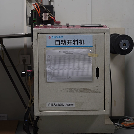
Flex Circuit Board Cutting
Customized size cutting can save costs:
First, the first step is material cutting. It is necessary to cut the board according to the data and design requirements provided by the customer, and cut the substrate material to the required size. After cutting, the substrate needs to be pretreated to remove the surface pollutants of copper film and improve the surface roughness, which is conducive to the subsequent film pressing process.
-
-
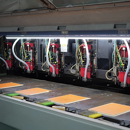
Flexible PCB Structure Layer formation
Lamination-Exposure Development-PTH Removal:
PCB, the inner layer shall be pressed first, and the copper surface of the finished substrate shall be pasted with an anti-corrosion dry film through hot pressing. Then, after exposure and development, the image on the original negative film is transferred to the photosensitive base plate through the action of the light source, and the dry film without chemical reaction is washed off with alkali solution, leaving the dry film with chemical reaction as the anti-corrosion protective layer during corrosion. The exposed copper after development is corroded by the drug solution to form the required inner line pattern.
-
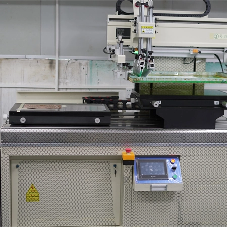
Troubleshoot FPC Defects Or Errors
Etching - Inner layer Inspection - AOI And VRS Confirmation:
After etching, the film needs to be removed, and the strong alkali is used to peel off the anti-corrosion layer on the protective copper surface to expose the circuit diagram. After the PCB proofing circuit is etched, it is necessary to check the inner layer, pick out the abnormal PCB for treatment, then punch through the CCD, and punch out the positioning hole and rivet hole of the detection operation with the CCD. The next step is AOI inspection and VRS confirmation. Using the principle of light reflection, the image is fed back to the equipment for processing, compared with the set logic judgment principle or data graphics to find out the abnormality. After connecting with AOI, the test data of each test version is transmitted to VRS through VRS, and the abnormality detected by AOI is confirmed manually.
-
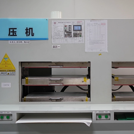
Multilayer Flex Circuit Board Proofing
Multilayer Lamination-Riveting-Surface Finishing:
After the inner board is confirmed to be correct, the next step is to press the copper foil, film and the oxidized inner circuit board into a multilayer board. After the pressing plate is finished, the copper surface needs to be browned and roughened. The surface area in contact with the resin on the copper surface is increased to increase the wetting of copper to the flowing resin, so as to blunt the copper surface and avoid adverse reactions. Then riveting is required, and multiple inner plates are nailed together with rivets to avoid sliding between layers in the subsequent processing process. After riveting, laminate the pre laminated floor into laminated multi-layer plate, and then press the laminated plate into multi-layer plate by hot pressing.
-
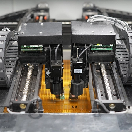
Up To 10 Layers Flex PCB Prototyping
Drilling-Plating-Exposure Imaging-Secondary Plating:
After the pressing is completed, the hole is drilled, and the through hole for the line connection between layers is drilled on the board surface. After drilling the hole is electroplating, so that the resin and glass fiber of the non-conductive part on the hole wall are metallized, and then the glue slag needs to be removed to expose the copper holes to be interconnected in each layer. Then, the outer layer needs to be treated, film pressed, exposed and developed, and then the secondary electroplating is carried out. The copper thickness is plated to the thickness required by the customer. After tin stripping, the line etching, AOI inspection and VRS of the outer layer are carried out. The more layers of flex PCB that customers need to proofing, the more pressing times and processes they need to perform.
-
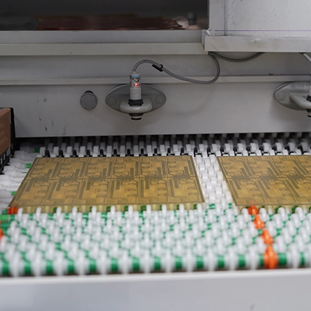
Protection Of Flexible PCB Samples
Solder Mask-Silk Screen-Manual Inspection-Sampling:
After checking and confirming that each layer is correct, anti welding is required to achieve the purpose of anti welding, protective plate and insulation, followed by silk screen characters for maintenance and identification.The final process is surface processing and manual testing. Of course, some customers will also have some special processes. In short, proofing is based on the specific information of customers.
-
Frequently Asked Questions and Answers
QA 1: How long does it take to proof a single-sided flexible circuit board?
It only takes 1-3 days for flexible boards and general-purpose circuit boards. Simple single-sided and double-sided layout soft board, proofing cycle 1-3 days.
QA 2: Does Best FPC provide free circuit board samples?
Yes, if the MOQ is more than 500pcs, we can provide free samples, and at the same time will print 10pcs more for regular delivery.
QA 3: How many layers of flexible circuit boards can you sample?
There is no big difference in the production process between PCB design and proofing. Best FPC can produce circuit boards with 1-10 layers. At the same time, it has its own SMT factory to complete the process of patch assembly, and solve the customer's circuit board needs in one stop.
QA 4: How long does it take for the Flexible PCB sample of Best FPC to be finished??
In addition to the number of layers of the PCB, the wiring density, application difficulty and material grade of the circuit board will directly affect the entire cycle of circuit board proofing. We go all out and can send flex board samples within 48-72 hours.
QA 5: Is the flex circuit board proofing done by your company independently?
Yes, as the original factory in Shenzhen, China, we can complete FPC design, prototyping and mass production services in one stop.
QA 6: How to calculate the cost of flexible circuit board proofing?
The circuit board sample fee depends on the number of layers, copper thickness, size, surface treatment and other parameters.

