


 2025-06-03
 BEST
BEST
Rigid-flex PCBs represent a sophisticated integration of rigid and flexible circuitry, offering unmatched versatility for modern electronic applications. Adhering to rigid flex PCB design guides ensures smooth transitions between rigid and flexible sections, preventing stress-related failures and enhancing reliability and performance. Specific design rules, such as defining proper bend radii, play a pivotal role in avoiding damage during operation, which directly impacts manufacturability. By following a comprehensive design rules document, designers can achieve PCBs that conform to the highest industry standards, balancing structural integrity with functional efficiency. This careful approach elevates rigid flex circuit design to meet both operational and manufacturing demands.
Key Takeaways
- Pick the right materials for stiff and bendy parts. Use FR-4 for stiff areas and polyimide for bendy ones to work better.
- Keep the layer stack balanced for strong structure. Spread stiff and bendy layers evenly to stop bending problems.
- Use good grounding methods to keep signals clear. Continuous ground planes block interference and make it work better.
- Measure the smallest bending radius carefully to avoid breaks. Follow the formula to keep it strong when bending.
- Work with manufacturers early while designing. This teamwork fixes problems early and makes building easier.
Material Selection for Rigid Flex PCB
Substrate Choices for Rigid and Flexible Sections
Selecting the right substrate is fundamental to achieving optimal performance in rigid-flex PCB designs. The rigid sections typically utilise materials like FR-4 epoxy glass, which offers excellent mechanical stability and electrical insulation. Flexible sections, on the other hand, often rely on polyimide due to its superior thermal stability and flexibility.
Polyimide substrates have become a preferred choice for rigid-flex PCBs, especially in industries like aerospace and automotive. Their ability to withstand harsh environments ensures reliability in applications requiring durability and compactness. For instance:
- A case study in aerospace demonstrated the successful use of rigid-flex PCBs in satellite communication systems, where polyimide substrates contributed to lightweight and compact designs.
- Automotive applications increasingly adopt rigid-flex PCBs to reduce weight and volume, enhancing fuel efficiency and meeting stringent design requirements.
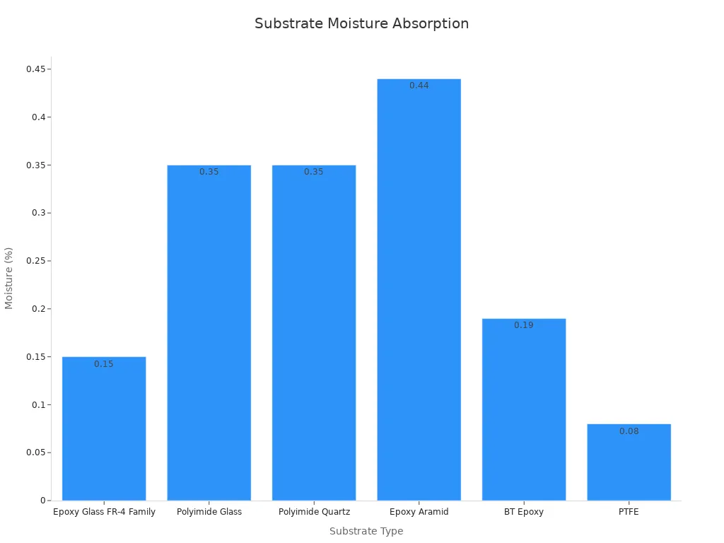
The table below compares common substrate types and their properties, aiding designers in selecting the most suitable material for their application:
| Substrate Type | Glass Transition Temperature (°C) | Coefficient of Temperature Expansion (X-Y) | Dielectric Constant at 1 MHz | Moisture Absorption (%) | Electrical Strength | Peel Strength Lbs./in | Applications |
|---|---|---|---|---|---|---|---|
| Epoxy Glass FR-4 Family | 135-210 | 13-17 | 4.4 – 4.8 | 0.15 | 1000-3000 | >2.0 | Computers, Backplanes |
| Polyimide Glass | 250 | 12-16 | 4.0 – 4.6 | 0.35 | N/A | >1.4 | Mobile Products |
| Polyimide Quartz | 250 | 6-8 | 3.5 – 3.8 | 0.35 | N/A | >1.2 | MEMS, Solar Cells |
| Epoxy Aramid | 180 | 7-9 | 3.8 - 4.1 | 0.44 | N/A | >1.7 | Avionics, Ultra-thin cell phones |
| BT Epoxy | 185 | 13-14 | 3.8 – 4.0 | 0.19 | 1200 | >2.0 | Microelectronics |
| PTFE | 188 | 60 | 2.75 - 3.0 | 0.08 | 1090 | >8.0 | RF/Microwave |
Adhesive Types and Their Role in Flexibility
Adhesives play a crucial role in rigid-flex PCB fabrication, ensuring the integrity of flexible sections while maintaining durability. The choice of adhesive impacts flexibility, adhesion strength, and heat resistance. Common adhesive types include acrylic, epoxy, polyester, and polyimide.
Polyimide adhesives are particularly favoured for their high thermal stability and mechanical flexibility, making them ideal for applications in harsh environments. A technical guide evaluating adhesive performance highlights key criteria such as:
- Adhesion strength to prevent delamination during bending.
- Thermal stability to withstand high temperatures during operation.
- Chemical resistance to ensure durability in challenging conditions.
The medical device industry benefits significantly from rigid-flex solutions, where adhesives enhance the durability and flexibility of advanced equipment. Designers must carefully evaluate adhesive properties to ensure compatibility with both rigid and flexible substrates.
Thermal and Mechanical Properties to Consider
Thermal stability and mechanical strength are critical in rigid-flex PCB design. Substrates must endure the heat generated during operation without degrading or altering their electrical properties. Materials with high thermal resistance prevent issues like warping or delamination, ensuring reliable performance.
The table below summarises key thermal and mechanical properties essential for rigid-flex PCB designs:
| Property | Description |
|---|---|
| Thermal Resistance | Validates thermal cycling performance during prototyping as per IPC-6013. |
| Mechanical Stability | Ensures reliability during bending as outlined in IPC-2223. |
| Bending Performance | Ability to withstand repeated bending without failure, critical for design. |
Rigid-flex PCBs integrate flexible and rigid substrates to meet stringent design guidelines, enabling complex circuitry in constrained spaces. Designers must prioritise materials with robust thermal and mechanical properties to ensure long-term reliability.
By selecting substrates and adhesives with optimal thermal and mechanical properties, designers can achieve rigid-flex PCBs that excel in performance and durability across diverse applications.
Layer Stack-Up in Rigid Flex PCB Design
Balancing Rigid and Flexible Layers
Achieving a well-balanced layer stack-up is critical in rigid flex pcb design. It ensures structural stability and prevents warping during fabrication and operation. Designers must carefully distribute rigid and flexible layers to maintain mechanical equilibrium. For instance, placing an equal number of layers on either side of the central plane reduces stress and minimises the risk of deformation.
Rick Hartley, a renowned expert in PCB design, highlights the importance of proper stack-up design to mitigate noise and signal integrity issues. His insights emphasise that a balanced stack-up not only enhances mechanical stability but also improves electromagnetic interference (EMI) control. This approach is particularly vital for rigid-flex pcbs used in high-frequency applications, where signal integrity is paramount.
To optimise the balance between rigid and flexible layers, designers should consider the following:
- Use symmetrical layer arrangements to distribute stress evenly.
- Avoid excessive thickness in flexible sections to maintain bendability.
- Ensure consistent material properties across layers to prevent thermal mismatches.
By adhering to these principles, rigid flex solutions can achieve superior performance and reliability, even in demanding environments.
Symmetry and Impedance Control
Symmetry plays a pivotal role in maintaining impedance control within multi-layer rigid-flex pcbs. Impedance mismatches can lead to signal reflections, resulting in degraded performance. To address this, designers must ensure that the stack-up remains symmetrical, particularly when routing high-speed signals.
When placing components like capacitors in series, symmetry rules must be followed to ensure impedance continuity. Differential pairs, commonly used in high-speed designs, require special attention. Designers should:
- Keep differential pairs as short as possible.
- Maintain consistent spacing between signal lines to control differential impedance.
- Minimise the number of vias to reduce signal distortion.
Simulation tools can help validate impedance control strategies during the design phase. These tools allow designers to model the effects of symmetry and spacing on signal integrity, ensuring that the final design meets performance requirements.
Signal Integrity in Multi-Layer Designs
Signal integrity is a cornerstone of rigid flex circuit design, particularly in multi-layer configurations. Poor signal integrity can result in data loss, increased noise, and reduced system reliability. To address these challenges, designers must focus on optimising via placement, ground plane continuity, and layer stack-up.
Industry reports highlight the impact of via design on signal integrity. Minimising the number of vias and optimising their placement reduces signal degradation. Ground planes also play a crucial role. Continuous ground planes enhance signal return paths, while multi-layer ground planes improve overall performance.
Designers should also collaborate with manufacturers during the fabrication process to ensure that the design aligns with production capabilities. This collaboration helps address design challenges early, reducing the risk of costly revisions.
By prioritising signal integrity, rigid-flex pcbs can deliver reliable performance across a wide range of applications, from consumer electronics to aerospace systems.
Bending Radius in Rigid Flex Circuit Design
Calculating Minimum Bending Radius
Determining the minimum bending radius is essential in rigid-flex pcb design to prevent mechanical stress and ensure long-term reliability. The bending radius defines the smallest curve a flexible section can achieve without compromising its structural integrity. Designers must account for material properties, trace thickness, and the number of conductive layers in bending areas.
A general rule of thumb suggests that the minimum bend radius should always be smaller than the intended bend radius to avoid stress-related failures. The neutral bending axis, which experiences no longitudinal stress, shifts depending on the radius and material composition. Thicker traces require greater overforming, increasing stress during bending.
The table below summarises standard and advanced minimum bending radius values based on the number of conductive layers:
| Conductive Layers in the Bend Area | Minimum Bend Radius (Standard) | Minimum Bend Radius (Advanced) |
|---|---|---|
| 1 layer | ≥ 5 mm | ≥ 3 mm |
| 2 layers | ≥ 7 mm | ≥ 5 mm |
For precise calculations, designers can use the formula:
G = (πR (A2) ÷ 180) + 4mm
Where G represents the minimum bend length, R is the inner bend radius, and A2 is the bending angle in degrees. The additional 4mm accounts for safety compensation derived from empirical values.
Avoiding Stress in Flexible Sections
Stress in flexible sections can lead to delamination, cracking, or electrical failures. Effective design techniques minimise stress and enhance the durability of rigid-flex pcbs. Designers should avoid sharp bends and ensure gradual transitions between rigid and flexible areas.
Case studies highlight successful strategies for stress reduction. A fitness tracker manufacturer improved reliability by using flexible pcbs to withstand mechanical stresses from daily use. Similarly, an automotive company enhanced the durability of instrument clusters by employing flex and rigid-flex pcbs, which resisted vibrations and temperature fluctuations. In medical devices, flexible pcbs improved manoeuvrability in endoscopic instruments, reducing the risk of failures.
To further mitigate stress, designers should:
- Use curved traces instead of sharp angles.
- Distribute stress evenly across bending areas.
- Avoid placing vias or components near high-stress zones.
Reinforcement Strategies for High-Stress Areas
High-stress areas in rigid flex circuit design require reinforcement to prevent premature failures. Stress-relieving mechanisms, such as optimised metallisation layers and meander designs, effectively distribute stress and delay failure points.
Research findings demonstrate the benefits of reinforcement strategies:
- Stretchable designs withstand elongation levels exceeding 315% and endure thousands of stretch-release cycles.
- Meander patterns lower peak stress values, enhancing durability.
- Multilayer approaches improve stress distribution across flexible circuits.
The table below summarises key findings from technical studies:
| Key Findings | Description |
|---|---|
| Stress Relief Mechanism | Metallisation layers and reinforcing elements reduce stress in critical areas. |
| Performance Metrics | Meander designs delay failure points and improve durability. |
| Stretchability | Designs endure extreme elongation and repeated cycles. |
| Future Directions | Multilayer approaches enhance stress distribution further. |
By implementing these reinforcement strategies, rigid-flex design achieves greater reliability and performance, even in demanding applications.
Trace Routing in Rigid Flex PCB Design
Best Practices for Trace Width and Spacing
Trace width and spacing significantly influence signal integrity and overall performance in rigid-flex PCB designs. Industry benchmarks recommend several best practices to optimise routing and minimise issues such as crosstalk and electromagnetic interference (EMI):
- Avoid hot spots by arranging vias in a grid pattern to prevent increased current density.
- Use 135° trace bends instead of 90° for high-speed signals to ensure smooth PCB etching.
- Increase the distance between signals outside bottleneck regions to reduce crosstalk.
- Implement daisy chain routing to eliminate long stub traces and maintain signal integrity.
Additionally, technical articles highlight the importance of horizontal spacing between adjacent traces. A minimum spacing of five times the vertical distance to the nearest reference plane (5H) is recommended for optimal performance. Designers should also consider material constraints and design intent when determining trace widths and air gaps.
Signal Interference in Flexible Areas
Signal interference poses unique challenges in flexible sections of rigid-flex PCBs. Controlled studies reveal that interference effects, such as response-related (RR) interference, can significantly impact signal performance. For example, RR interference increases reaction time costs during task switching, as observed in fMRI studies. This phenomenon underscores the importance of mitigating interference in bending areas.
To address these challenges, designers should prioritise short, direct traces between components and avoid routing signals near high-stress zones. Routing traces vertically on one side of the board while maintaining horizontal routing on the opposite side can further minimise interference. These strategies enhance signal integrity and ensure reliable performance in flex PCB designs.
VIA Placement Guidelines
Optimal VIA placement is crucial for maintaining connectivity and structural integrity in mixed PCB sections. Empirical testing provides valuable insights into VIA types and their conditions for use:
| VIA Type | Conditions for Optimal Use | Aspect Ratio | Annular Ring Size | Notes |
|---|---|---|---|---|
| 20/10mil | Regular multilayer board, BGA pitch of 0.8mm or more, enough board space for regular vias | 1:6.4 | 5mil | Stronger structure, suitable for class 2 design, increase annular ring in less dense areas |
| 22/12mil | Low cost 2 layer PCBs, thick PCBs with high layer count | 1:10 | N/A | Widely used, easily fabricated |
| 18/8mil | Up to 1.6mm board thickness, used in dense areas | 1:8 | 5mil | More fragile than 20/10mil, use only when necessary |
| 16/8mil | Not recommended due to small annular ring | N/A | 4mil | Technically feasible but not advisable due to clearance issues |
| 16/6mil or 14/6mil | Maximum board thickness of 1mm, aspect ratio of 1:6.7 | 1:6.7 | N/A | Smallest finished hole, generally not recommended |
Designers should select VIA types based on board thickness, layer count, and application requirements. For dense areas, smaller VIA sizes like 18/8mil may be necessary, though they are more fragile. Larger VIA types, such as 20/10mil, offer greater structural strength and are ideal for less dense regions.

By adhering to these guidelines, rigid-flex design achieves enhanced connectivity and durability, ensuring reliable performance across diverse applications.
Ground Plane Design in Rigid Flex PCB
Signal Integrity with Proper Grounding
Proper grounding is essential for maintaining signal integrity in rigid-flex pcbs. Ground planes act as a conductive shield, isolating circuit components and minimising electromagnetic interference (EMI). They provide a stable reference potential, ensuring consistent signal performance across rigid and flexible sections. This is particularly critical in high-frequency applications, where even minor impedance mismatches can degrade signal quality.
Incorporating dedicated ground planes, ground vias, and galvanic isolation enhances the reliability of rigid-flex pcb designs. These techniques reduce noise and prevent unwanted coupling between traces. For instance, a ground plane offers a low-impedance path for return currents, minimising loop areas and reducing inductance. This approach not only improves signal clarity but also ensures compliance with design guidelines for high-performance pcbs.
Ground Plane Continuity Across Sections
Maintaining ground plane continuity across rigid and flexible sections is vital for achieving optimal performance in rigid-flex pcb designs. Disruptions in the ground plane can lead to signal reflections, increased noise, and compromised functionality. Designers must ensure that the ground plane remains uninterrupted, even in bending areas, to preserve signal integrity.
One effective strategy involves using overlapping ground planes at the transition points between rigid and flexible sections. This technique ensures a seamless connection, reducing the risk of EMI and crosstalk. Additionally, placing ground vias strategically along the transition zones enhances electrical connectivity and mechanical stability. Simulation studies have demonstrated that continuous ground planes significantly reduce interference, confirming their importance in flex pcb design.
Minimising EMI and Crosstalk
Electromagnetic interference and crosstalk pose significant challenges in rigid-flex pcb design. These issues can disrupt signal transmission, leading to data loss and reduced system reliability. Proper grounding and shielding techniques play a crucial role in mitigating these effects.
Simulation studies on various cable types, including coaxial and twisted pair cables, highlight the effectiveness of grounding in reducing EMI and crosstalk. Highly shielded designs, such as those with continuous ground planes, reject interference and maintain signal clarity. For example, simulations identified a resonance at 65 MHz, which was experimentally verified, demonstrating the accuracy of these methods in predicting EMI behaviour.
To minimise EMI and crosstalk, designers should prioritise the use of continuous ground planes, maintain adequate spacing between traces, and avoid routing signals near high-stress zones. These practices align with industry standards and ensure that rigid-flex pcbs deliver reliable performance in demanding applications.
Software Tools for Rigid Flex PCB Design
Features to Look for in PCB Design Software
Selecting the right software is crucial for achieving efficient and accurate rigid-flex pcb design. Modern tools offer a range of features that streamline the design process and enhance simulation accuracy. Key functionalities to consider include:
- Impedance-controlled routing to meet the specific requirements of high-speed circuits.
- Advanced simulation capabilities, such as parasitic extraction, EMI simulations, and heat transport analysis.
- Design rule checks (DRC) to identify potential errors, including trace overlap and unconnected nets.
- Electrical rule checks (ERC) to ensure circuit functionality by detecting power/ground shorts and signal integrity issues.
- Signal integrity analysis tools for evaluating trace impedance, signal reflection, and crosstalk.
- 3D visualisation for verifying physical layouts, identifying mechanical conflicts, and simulating assembly.
These features not only improve design accuracy but also reduce the likelihood of costly revisions during manufacturing. Designers should prioritise tools that integrate these capabilities to ensure compliance with design guidelines and industry standards.
Popular Tools for Rigid Flex Circuit Design
Several software solutions stand out for their ability to handle the complexities of rigid-flex pcb design. Tools like Ansys Sherlock and SimScale offer unique advantages:
| Feature | Ansys Sherlock | SimScale |
|---|---|---|
| User Interface | Specialised for electronics reliability simulation | User-friendly, accessible from any web browser |
| Unique Features | Focus on predicting failures of electronic components | Cloud-based access, real-time collaboration |
| Multi-Physics Simulation | Available through broader suite | Accessible without powerful local resources |
SPICE also remains a popular choice due to its detailed simulation capabilities. Advanced features like Monte Carlo Analysis and Parameter Sweeping make it ideal for high-reliability applications. These tools empower designers to optimise their pcbs for performance and durability.
Simulation Features for Design Validation
Simulation plays a pivotal role in validating rigid-flex pcb designs before manufacturing. Studies have shown that dynamic layout optimisation through simulation improves spatial efficiency and production capacity. Key simulation features include:
- Heat generation and transport simulations to evaluate thermal performance.
- CFD simulations for airflow visualisation in cooling systems.
- Mechanical vibration and fatigue simulations to assess durability.
- Network parameter simulations to account for parasitics in high-speed designs.
Strategic use of these simulations enhances product and process development, leading to better business metrics and a deeper understanding of design functionality. By leveraging these tools, designers can ensure their flex pcb design meets both performance and manufacturability requirements.
Design for Manufacturing in Rigid Flex PCB Design
Ensuring Manufacturability
Designing rigid-flex PCBs with manufacturability in mind ensures smooth production and reduces the risk of costly revisions. Adhering to established design guidelines is critical for achieving high manufacturability. For instance, consulting with fabricators about material choices based on bend types—dynamic or stable—can prevent failures during operation. Dynamic bends typically require a minimum bend radius of 100 times the material thickness, while stable bends can accommodate up to 20 layers with a radius of 10 times the material thickness.
The table below summarises key manufacturing guidelines:
| Guideline Category | Details |
|---|---|
| Material Considerations | * Consult with the manufacturer about materials depending on bend type. |
| Use of Corners and Teardrops | * Use curved corners and teardrops in flex areas to enhance joint strength. |
| Plated Through Holes | * Avoid plated through holes in bend areas to prevent structural weaknesses. |
| Routing Across Bending Area | * Maintain straight, perpendicular traces across bending areas. |
| Ground Plane Considerations | * Use cross-hatched ground planes in flexible areas to maintain flexibility. |
These practices not only improve manufacturability but also enhance the durability and performance of rigid-flex PCBs.
Addressing Common Manufacturing Challenges
Manufacturing rigid-flex PCBs presents unique challenges that require careful planning. Approximately 42% of manufacturers producing high-risk devices invest heavily in clinical evaluation training, compared to only 10% for medium-risk devices. This disparity highlights the importance of expertise in addressing complex manufacturing requirements.
Common challenges include:
- Ensuring consistent quality across rigid and flexible sections.
- Avoiding delamination during bending operations.
- Managing costs for small and medium enterprises (SMEs) that lack in-house expertise.
About 74% of manufacturers generate their Clinical Evaluation Reports (CERs) internally, reflecting a preference for leveraging internal knowledge. However, SMEs often face financial constraints when outsourcing such tasks, which can limit innovation. Addressing these challenges requires collaboration with experienced fabricators and adherence to robust design guidelines.
Collaborating with Fabricators
Collaboration between designers and fabricators is essential for optimising rigid-flex PCB design and manufacturing. Effective communication ensures that designs align with production capabilities, reducing errors and improving efficiency. Supply Chain Collaboration (SCC) has been shown to enhance performance metrics, with higher maturity levels linked to better outcomes.
The table below outlines collaborative methods and their impact:
| Collaborative Method | Performance Metric | Findings |
|---|---|---|
| Supply Chain Collaboration | Maturity Level | Higher levels of performance with effective SCC. |
| Internal Collaboration | Performance Outcomes | Moderates the relationship between external integration and performance. |
Designers should involve fabricators early in the process to address potential issues, such as material selection and layer stack-up. This proactive approach fosters innovation and ensures that rigid-flex PCBs meet both functional and manufacturability requirements.
Adhering to rigid-flex PCB design rules ensures reliable and efficient PCBs for diverse applications. These guidelines promote cost-effective development, reduce board size, and optimise bending performance. Key takeaways include selecting appropriate materials, maintaining balanced stack-ups, and ensuring proper grounding. Rigid-flex PCBs eliminate connectors, enabling compact, lightweight designs suitable for small devices. Their high thermal resistance and flexibility allow circuits to bend without deformation, enhancing durability. Designers should consult manufacturers early to align designs with production capabilities, minimising delays and reworks. Applying these principles leads to high-quality, dependable products.
FAQ
What is the primary advantage of rigid-flex PCBs?
Rigid-flex PCBs combine the durability of rigid boards with the flexibility of flexible circuits. This integration eliminates connectors, reduces assembly complexity, and enables compact designs. Their adaptability makes them ideal for applications requiring lightweight and space-efficient solutions.
How can designers calculate the bending radius for flexible sections?
Designers use the formula G = (πR (A2) ÷ 180) + 4mm, where G represents the minimum bend length, R is the inner bend radius, and A2 is the bending angle. This calculation ensures structural integrity during bending operations.
.png)
.png)
.png)
.png)

.png)

