


 2025-12-19
 BEST
BEST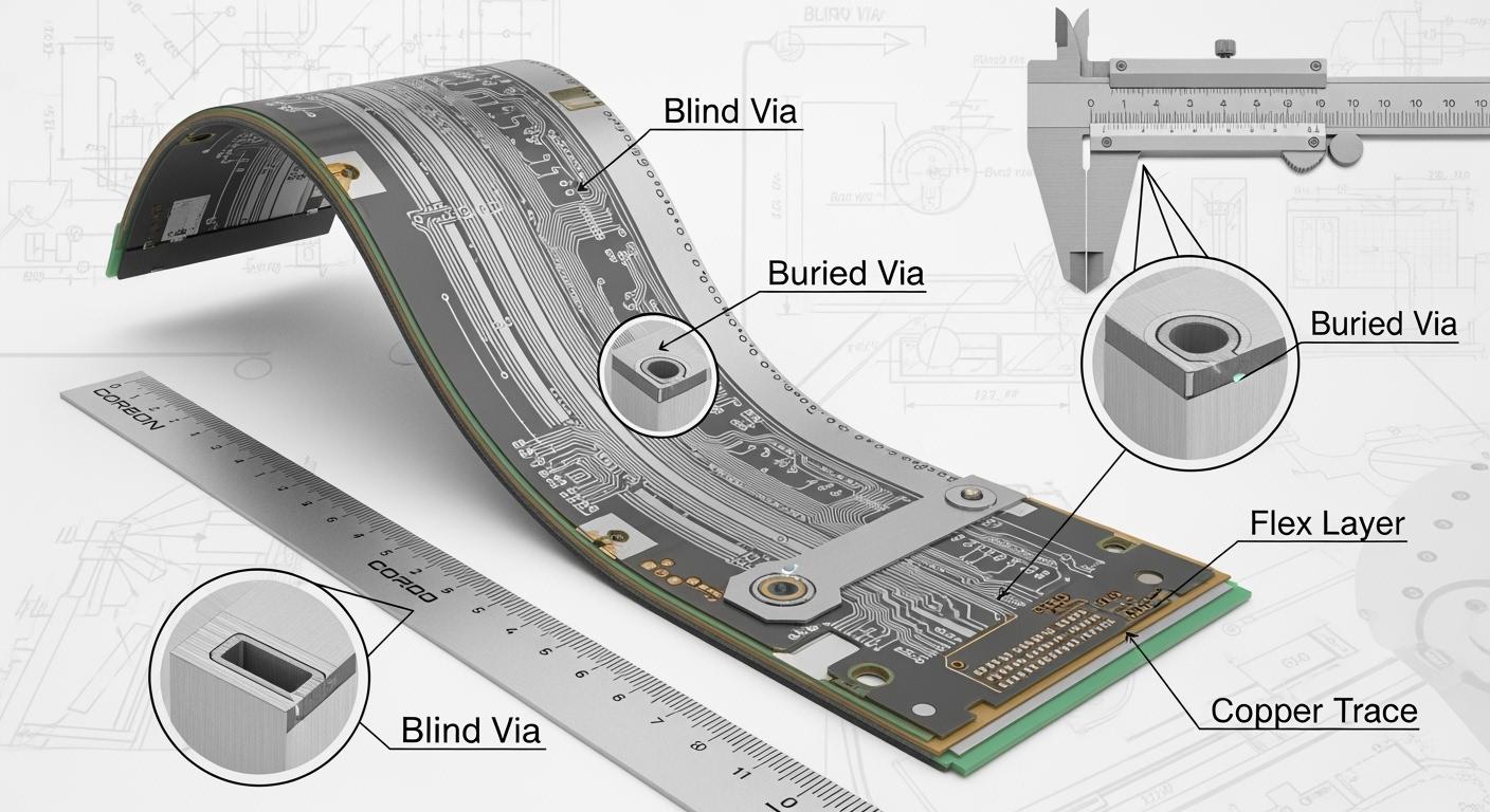
You can make your Blind buried hole FPC easier to build and more dependable by using good design tips. Pick the correct hole size and aspect ratio so you do not get problems. Make a different drill file for each hole type so makers know what you want. Set up design rules in your layout software so you do not make spacing mistakes. Careful planning saves money and stops common errors.
- Always make the hole diameter the same as the drill diameter.
- Do not route through too many layers so it works well.
- Use smart design to save space and money.
Take simple steps to get a good FPC design.
Key Takeaways
- Pick the correct hole size and aspect ratio to stop problems. Make sure the hole diameter matches the drill diameter for better results.
- Think about your layer stackup before you start. Try not to route through too many layers to make building easier and cheaper.
- Set simple design rules in your software for spacing and annular rings. This helps stop short circuits and weak spots.
- Talk clearly with your manufacturer. Give them diagrams and drill files early so you can find problems sooner.
- Look closely at DFM feedback. Change your design if needed so it can be made easily and does not cost too much.
Blind Buried Hole FPC Basics
What Are Blind and Buried Holes
Flexible printed circuits can have two special kinds of holes. Blind holes connect the top layer to inside layers. They do not go all the way through the board. Buried holes are found between inside layers only. They never reach the top or bottom. These holes help make tricky connections. They keep the board from getting too crowded.
Tip: Blind holes let you save space on the top. Buried holes hide connections inside the board.
When to Use Each Type
Blind holes are good for linking parts on the surface to inside layers. They work well when you need lots of connections close together. Buried holes are best for joining inside layers without touching the top. You use buried holes in boards with many layers. They give you more ways to route connections.
Here is a simple table to help you choose:
| Hole Type | Best Use Case | Surface Access |
|---|---|---|
| Blind | Connect surface to inner layer | Yes |
| Buried | Link inner layers only | No |
Key Benefits for FPCs
Blind and buried holes give you many good things in your Blind buried hole FPC designs:
- You save space on your board.
- You make signal paths better and lower noise.
- You build circuits that last longer and are easier to make.
- You lower the chance of short circuits.
Picking the right hole type helps your project work better and cost less. Good planning stops mistakes and makes sure your FPC does what you want.
Blind Buried Hole FPC Design Tips
Layer Stackup Planning
You need to plan your layer stackup before you start your Blind buried hole FPC design. Decide which layers will use blind holes and which will use buried holes. This step helps you avoid routing signals through too many layers. When you keep the number of layers low, you make the FPC easier to build and more reliable. Use a clear stackup diagram. Share this diagram with your manufacturer early in the process.
Tip: A simple stackup reduces cost and improves yield.
Hole Size and Aspect Ratio
Choose the right hole size for your Blind buried hole FPC. The hole diameter should match the drill diameter. Keep the aspect ratio (hole depth to hole diameter) at 1 or less. If you use a higher aspect ratio, you risk poor plating and weak connections. Always check your manufacturer’s limits for hole size and aspect ratio.
- Example: For a 0.2 mm thick board, use a 0.2 mm hole diameter.
Pad and Annular Ring
Design each pad with enough annular ring around the hole. The annular ring is the copper area that surrounds the hole. If the ring is too small, you may get open circuits or weak joints. Follow your manufacturer’s minimum ring size. A typical value is 0.1 mm or more. Use your PCB design software to set these rules.
Note: A strong annular ring improves reliability.
Spacing and Clearance
Set proper spacing between holes, pads, and traces. This step prevents short circuits and makes your Blind buried hole FPC easier to manufacture. Use your design software to set minimum clearance rules. Check your manufacturer’s guidelines for spacing. More clearance means fewer errors during production.
- Minimum spacing example: 0.15 mm between holes and traces.
Material and Flexibility
Pick materials that match your FPC’s flexibility needs. Polyimide is a common choice for Blind buried hole FPC designs. It bends well and handles heat. Make sure the adhesive and coverlay also support bending. If you use stiffeners, place them away from areas with blind or buried holes. This keeps the FPC flexible and strong.
Tip: Flexible materials reduce stress on vias and improve product life.
Via Filling and Plating
Decide if you need to fill or plate your vias. Filled vias give you a flat surface and protect the hole from moisture. Plated vias improve electrical connection and strength. Ask your manufacturer about their via filling and plating options for Blind buried hole FPC. Use separate drill files for each hole type to avoid confusion.
- Always review the finished via quality before final approval.
Common Pitfalls to Avoid
Frequent Design Mistakes
When you design blind buried hole FPCs, you can make some common mistakes. These mistakes can slow down making the board. They can also make it cost more or not work well. Here are the most common problems:
- Improper Aspect Ratio: Sometimes, the hole is too deep for its width. This can make the plating bad and the connection weak.
- Excessive Layer Routing: If you send signals through too many layers, building the FPC gets harder. This can cause more problems and make it less reliable.
- Unclear Drill Files: If you do not make different drill files for each hole type, the maker might get confused. This can put holes in the wrong place.
- Insufficient Annular Ring: If the ring around the hole is too small, the circuit can break or be weak.
- Tight Spacing: If holes, pads, or traces are too close, you can get short circuits or mistakes when making the board.
⚠️ Tip: Always look for these mistakes before you send your files to the maker.
Solutions and Best Practices
You can stop these problems by using smart steps. Try these best ways to make your blind buried hole FPC better:
| Mistake | Solution |
|---|---|
| Improper Aspect Ratio | Keep aspect ratio ≤ 1. Confirm with manufacturer. |
| Excessive Layer Routing | Limit routing to essential layers only. |
| Unclear Drill Files | Create separate drill files for each hole type. |
| Insufficient Annular Ring | Set minimum ring size in design software. |
| Tight Spacing | Follow manufacturer’s spacing guidelines. |
- Check your stackup and routing before you finish the design.
- Use your PCB software to set rules for holes, rings, and space.
- Talk to your maker early. Ask them to check your files.
- Look at your drill files and layer pictures to make sure they are clear.
✅ Best Practice: Check every part of your design two times. Good planning saves you time and money.
Working with Manufacturers
Clear Communication
It is important to talk clearly with your manufacturer. This helps you stop mistakes and delays. Share your stackup diagrams early in the process. Give them your drill files and design rules too. This lets your manufacturer know what you need. They can find problems before making your FPC.
- Send drill files for blind holes and buried holes.
- Give layer diagrams that show each part.
- List all design rules for spacing, hole size, and annular ring.
.png)
.png)
.png)
.png)

.png)

