


 2025-08-22
 BEST
BEST
You should use important DFM strategies for flex pcb design. This helps you make products that work well and cost less. It also makes them easier to build in 2025. Data shows DFM checking algorithms now find 98% of flex pcb problems during design. AOI integration has made prototype times almost half as long. When you use DFM Flexible Circuits methods, you make placing parts and routing easier. This lowers mistakes and saves time. Good documentation and teamwork with manufacturing partners help your flex pcb meet quality goals and industry rules.
Key Takeaways
- Pick flexible materials like polyimide and rolled annealed copper. These help your flex PCB stay strong and bend easily.
- Follow bend radius rules to stop breaks. Use smooth curves. Do not use sharp bends in flexible zones.
- Design traces and vias with care. Keep enough space between them. Do not put vias in bend areas. Use teardrop pads to lower stress.
- Put stiffeners only outside flex zones. This helps support heavy parts and connectors. It does not make the board less flexible.
- Work with your manufacturer closely. Use clear documents. Do DFM checks and tests early. This helps find problems and keeps quality high.
DFM Flex PCB Overview
Why DFM (Design for Manufacturability) Matters
It is important to use dfm flex pcb strategies. This helps your flex pcb work well and makes building easier. Design for manufacturability lowers mistakes and makes your flex pcb more reliable. Flex and rigid-flex pcbs have special problems. You need to follow dfm rules for flexible circuits to stop issues during assembly and testing.
Here are the main ideas for dfm flex pcb:
- Pick parts that fit what manufacturers can do and use standard footprints.
- Make the layout simple for assembly and good for heat control.
- Add things for heat control, like heat sinks and thermal vias.
- Put in test points and self-test features to find faults easily.
- Make sure your design follows industry rules and standards.
- Use lessons from old projects to make your next flex pcb better.
Tip: Doing dfm checks early and often helps you find problems before they cost a lot. Special dfm software tools can look at your flex pcb design and help stop mistakes.
Group parts by how much stress they can take. Use flexible leads and give extra space for movement. Use standard footprints and pick common parts to make assembly simple. Always check your design with design rule checks. Keep your flex pcb easy by using fewer vias and layer changes.
Key Challenges in 2025
In 2025, FPC pcb manufacturing will have new problems. Devices are getting smaller and stronger, so heat control is harder. You need better heat sinks and materials that move heat well. FPC pcbs must last in tough places, like high heat and strong shaking. Pick materials and designs that make them stronger.
Bendable pcb costs are still higher than rigid pcbs. The industry is trying new ways and machines to lower these costs. You must watch temperature and pressure during lamination to stop warping or delamination. Drilling and making vias is hard because flexible materials can rip. Laser drilling helps but costs more. Testing is harder too. You may need X-ray or special tests to check inside layers and make sure your flex pcb can bend many times.
Work with your manufacturer to set up testing steps. Use adhesive-less polyimide and rolled annealed copper for better bending. Route traces in curves and stagger layers to spread out stress. Do not put vias in bend areas and keep tight tolerances to stop shorts or opens. Following dfm rules for flexible circuits and design for manufacturing rules will help you solve these problems and make strong flex pcbs.
Material Selection
Substrate Choices
You have to pick the right substrate for your flexible circuit boards. Polyimide is the most common material for flexible pcbs. It lets the board bend and fit into tight spots. Polyimide is used in things like smartwatches, foldable phones, and medical tools. Flexible circuit boards are in many new gadgets. They help save space and make things lighter.
Here is a table that shows how much each substrate is used in pcbs:
| Substrate Material Type | Description / Notes | Market Share (2023) |
|---|---|---|
| Flexible PCB Substrates | Mostly polyimide films; they bend and fit in small places | 25% |
| Rigid PCB Substrates | FR-4, CEM-1, CEM-3, epoxy, ceramic, metal-based; used in hard pcbs | 75% |
Polyimide can handle heat and keeps electricity from leaking. PTFE and PEEK are used for special needs. PTFE is good for high-frequency signals. PEEK stands up to chemicals and high heat. Polyimide works well for single-sided flexible pcbs. Rigid-flex substrates mix flexible and hard layers for strength and bending. These choices help flexible pcbs work in advanced electronics.
Note: More people want flexible substrates because wearable and mobile devices are popular.
Reliability Factors
You need to think about reliability when picking materials for flex pcbs. Polyimide can take high heat and bend without breaking. Adhesiveless substrates help stop layers from peeling apart. Rolled annealed copper bends better and keeps traces safe. Single-sided flexible pcbs bend more and fail less.
- Temperature resistance: Materials must handle high heat.
- Mechanical stress tolerance: Boards should bend many times and not break.
- Chemical resistance: Substrates must not get damaged by water or chemicals.
- Electrical properties: Low dielectric loss keeps signals strong.
- Flexibility and mechanical reliability: Good bend radius stops cracks.
- Adhesive vs. adhesiveless: Adhesiveless laminates work better.
- Copper foil type: Rolled annealed copper is best for flexible pcbs.
- Protective coatings: Coverlays and coatings keep out water and chemicals.
You should test flexible circuit boards for bending, shaking, hits, and wetness. Make sure the substrate and parts expand the same way with heat. Use AOI and X-ray checks to find problems early. Work with your manufacturer to improve your design and material stack. These steps help flexible pcbs last longer and work better.
Flex PCB Design Essentials
Bend Radius
You must think about bend radius when you design flex pcbs. Bend radius means the smallest curve your flex pcb can handle. If you bend it too much, copper traces might break or peel off. Always figure out the minimum bend radius for your flex pcb. This depends on how thick it is and how many layers it has. The IPC-2223 standard tells you the right rules to follow.
Here is a table that shows the best bend radius for each flex pcb type:
| Flex PCB Layer Count | Static Flex Minimum Bend Radius (× thickness) | Dynamic Flex Minimum Bend Radius (× thickness) |
|---|---|---|
| Single Layer | 10 | 100 |
| Double Layer | 10 | 150 |
| Multi-Layer | 20 | Not recommended |
For example, if you have a single-layer dynamic flex pcb that is 0.2 mm thick, you need a bend radius of 20 mm. Multi-layer flex pcbs should not be used for lots of bending. If you only bend it once, you do not need a strict bend radius. Use thin materials and put copper near the middle to lower stress.
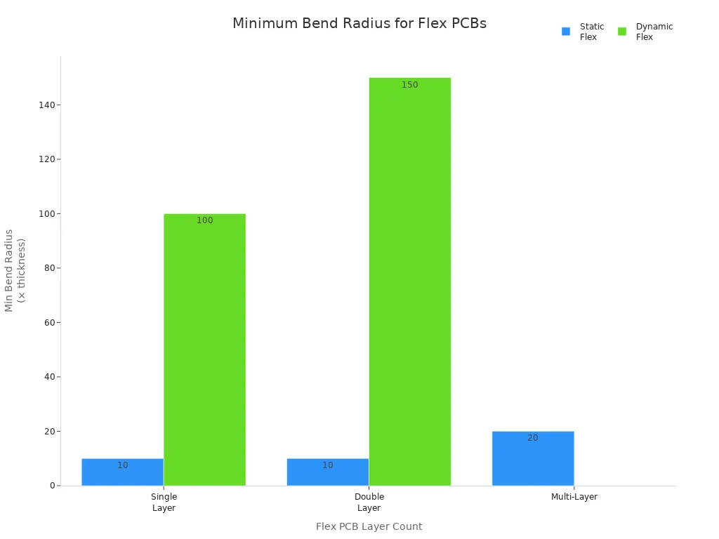
Tip: Always use these bend radius rules in your flex pcb design. This helps stop breaks and keeps your flex pcb working well.
Flex Zones
Flex zones are the parts of your flex pcb that bend or move. You need to design these areas with care so your flex pcb stays strong. Copper can bend many times because it is tough and flexible. Put copper layers close to the middle to lower stress and stop cracks. How you stack the layers is important too. If layers are too far apart, stress goes up. If they are too close, the board will not bend as well.
- Pick polyimide for flex layers because it bends and handles heat.
- Make trace routing easy in flex zones. Use wide traces and more space. Do not make sharp turns.
- Put vias at least 1.27 mm away from where flex meets rigid.
- Follow bend radius rules: 10× thickness for static bends, 20× or more for dynamic bends.
- Add stiffeners at transition spots to stop peeling.
- Use cross-hatched ground planes in moving zones for better bending.
- Thinner flex pcbs bend more but may break sooner. Thicker spots make the board stronger.
Flex zones help your flex pcb last longer in hard places. You find flex pcbs in medical, car, airplane, and home electronics. Good flex zone design keeps your flex pcb working after many bends.
Trace & Via Design

Trace Width & Spacing
You have to pick the right trace width and spacing. Trace width decides how much current your flex pcb can handle. Wider traces help stop overheating. This keeps your flex pcb safe. Spacing between traces stops shorts. It also keeps signals clear. You need to follow industry rules. This makes sure your flex pcb works well and passes safety checks.
Here is a table that shows the smallest space between traces for different pcb classes and voltage levels:
| PCB Class / Voltage Level | Minimum Trace-to-Trace Spacing |
|---|---|
| Class 2 (Low Voltage) | 0.25 mm (10 mil) |
| Class 2 (High Voltage) | 0.5 mm (20 mil) |
| Class 3 (Low Voltage) | 0.15 mm (6 mil) |
| Class 3 (High Voltage) | 0.5 mm (20 mil) or more |
You should think about creepage and clearance distances too. These can be from 0.1 mm to 2 mm. The amount depends on voltage and pcb class. UL 796 and IPC-2221 give rules for spacing and safety. Differential pair spacing should be 0.1x to 0.3x trace width. This helps keep signals strong. Some manufacturers can make very thin traces, like 0.035 mm. Always check with your supplier before you finish your design.
Tip: Talk to your manufacturer early. This helps match your flex pcb design to what they can do. It lowers mistakes and helps you get better results.
Via Types
You need to pick the right via types for your flex pcb. Vias link layers and let signals move through your pcb. The kind and spot of vias change how strong and easy to build your pcb is. Through-hole vias are used in double-sided pcbs. They are simple to make. But they can have high aspect ratios. This may cause plating problems and signal loss. Blind and buried vias only link some layers. These have lower aspect ratios. This helps plating and signal quality.
Microvias are best for high-density and high-speed flex pcb designs. They are small and have low aspect ratios. This makes them strong and easy to build. Advanced via methods, like filled and capped vias, backdrilled vias, and laser microvias, help lower defects and boost performance. Do not put vias in flex zones. This stops stress and keeps your flex pcb from breaking when bent many times.
- Do not put vias or parts in places that bend a lot.
- Use blind or buried vias to keep them out of bending spots.
- Add strain reliefs to important areas.
- Follow DFM rules for trace width, spacing, and layer stack-up.
- Use AOI and electrical tests to find problems early.
Note: Making via design and layout better helps your flex pcb last longer and work well. Work with your manufacturer to pick the best via types for your needs.
Layer Stack-Up
Construction Types
You have to pick the right stack-up for your flexible circuit boards. The stack-up tells you how many layers your board has. It also shows how the layers work together. Each type is good for different things like strength, routing, or bending.
- Single-layer stack-ups have one copper layer on polyimide. These are in single-sided flexible pcb designs. They are good for simple circuits that need to bend a lot.
- Double-layer stack-ups have copper on both sides of the board. This helps signals and gives more ways to route traces. It also lets you add ground planes for better performance.
- Four-layer stack-ups give you more space for routing and still bend well. You find these in flex and rigid-flex pcbs for harder designs. They put signal layers between power and ground planes to control signals and stop noise.
- Six-layer or more stack-ups are for advanced systems. These need careful design and special ways to make them. They help with routing and control electromagnetic problems.
- Rigid-flex stack-ups mix flexible and hard parts. You use these when you want both strength and bending. You must plan carefully where the flexible and hard parts meet.
- Adhesiveless stack-ups do not use glue. This makes the board thinner and stronger. They work well in tough places.
You can choose ultra-thin, thin, or thick flexible circuit boards. Ultra-thin boards are less than 0.1 mm thick and fit in tiny devices. Thin boards are from 0.14 mm to 0.2 mm thick. Thick boards can be up to 1.0 mm for more strength. The thickness of copper and polyimide also changes how much your board can bend.
Tip: Always pick a stack-up that matches your device’s needs. This helps your flexible circuit boards last longer and work better.
Laminate Selection
You need to pick the right laminate for your flexible circuit boards. Polyimide laminates are best for most flexible designs. They can take high heat and do not get hurt by chemicals. This keeps your board safe in many places.
Polyimide gives strong support and lets your board bend many times. It also keeps signals safe because it has a good dielectric constant and stops radiation. You should not use FR-4 laminates for flexible or high-frequency uses. FR-4 does not bend well and loses more signal.
Here is a table that shows how laminate properties change your board:
| Property Category | Property Name | Impact on Flexible Circuit Boards |
|---|---|---|
| Electrical | Dielectric Constant | Controls signal speed and keeps signals clear at high frequencies. |
| Electrical | Dielectric Loss | Lower loss means better signal quality for fast circuits. |
| Mechanical | Peel Strength | Stops layers from peeling when you bend the board. |
| Mechanical | Flexural Strength | Lets your board bend without breaking. |
| Mechanical | Dimensional Stability | Keeps your board the right size and shape during use. |
You should also check how much water the laminate takes in. Low rates (0.01% to 0.2%) help your flexible circuit boards keep their shape and work well. The right laminate gives your single-sided flexible pcb and flex and rigid-flex pcbs the best mix of strength, bending, and electrical performance.
Assembly & SMT
Assembly Techniques
You have to use the right ways to put together flex PCBs. Flex PCBs can bend and move, so you need strong methods. Surface Mount Technology (SMT) is used the most. Small parts are put on the board by machines. This way is fast and good for making lots of boards. It works well for designs with many parts close together.
Adhesive bonding is used when you need more bending. Special glue holds layers or parts together. This keeps the board from breaking when it bends. Robots can also put and solder parts very quickly. This makes building many boards faster and easier.
Here is a table that shows the best ways to put together flex PCBs:
| Technique | Description | Advantages |
|---|---|---|
| Surface Mount Technology (SMT) | Small parts are placed by machines on flexible boards | Fast, good for making many boards |
| Adhesive Bonding | Glue is used to stick parts and layers together | Keeps board bendy, helps when SMT is not enough |
| Automated Assembly | Robots put and solder parts with great speed and care | Makes work faster, better, and bigger scale |
Making flex PCBs can be hard because they bend and move. You need special tools to handle them gently. Machines with cameras help put parts in the right place. Reflow soldering uses heat to make strong joins. Some ways to connect are Anisotropic Conductive Film (ACF) for screens, Zero Insertion Force (ZIF) connectors for hard boards, and hot bar soldering for connectors. Roll-to-roll making lets you build many boards without stopping, which saves time and money.
Checking quality is important at every step. You use Automated Optical Inspection (AOI), X-ray checks, and electric tests to find problems and make sure the flex PCB works.
Equipment Needs
You do not need special SMT machines for flex PCBs. You use normal machines like pick-and-place units, reflow ovens, and printers for solder paste. The big difference is how you handle the soft boards. You must change clamps and belts to keep the boards safe.
Normal SMT machines are fast pick-and-place units, ovens for heating, and machines to check solder paste. AOI and in-circuit testers are also used. These tools work for both hard and flex PCBs. Workers must learn to handle flex boards carefully. You also change the process to keep boards from getting hurt.
Laser Direct Imaging (LDI) helps make tiny patterns on the board. High-Density Interconnect (HDI) lets you use small vias and fit more parts. Roll-to-roll making helps build many boards and keeps costs down. You must keep the work area clean and pick the right materials to stop bending and keep boards flat.
Tip: Always talk with your factory partner to set up the best machines and steps for your flex PCB job. This helps you avoid mistakes and get good boards.
Documentation
Good and clear documentation helps you stop expensive mistakes. If you make careful design files, your manufacturer knows what you want. This lowers errors and keeps your project moving forward.
Design Files
You must give all the important design files and notes. These help your manufacturer build your flex PCB the way you want. Here are the main things you should include:
- Drawings for making and putting together the board with easy steps.
- A Bill of Materials (BOM) with right part numbers.
- Details about layer stackup, like what materials and thicknesses you use.
- Drill tables and size drawings with clear points to measure from.
- Gerber files, drill files, and specs for each layer.
- Design Rule Check (DRC) reports to show you looked for mistakes.
- Notes about soldermask, silkscreen, and marking needs.
- Steps for electrical testing and checking quality.
- Instructions for packing and shipping the boards.
Tip: Always use IPC standards like IPC-6013 and IPC-2223 in your files. This helps you follow rules and makes building easier.
Verification Steps
You need to check your design before you start making boards. Good checks help you find problems early and make your board work better. Use this list to help you:
- Mark which areas will bend and which will stay stiff.
- Do not put parts, vias, or plated through-holes in places that bend.
- Use the right bend radius for static and dynamic flex spots.
- Route traces with smooth curves and do not use sharp turns.
- Add stiffeners to hold connectors and stop bending near important parts.
- Put tooling holes and fiducials to help line up parts during assembly.
- Keep trace widths the same and stagger traces in bend areas.
- Make test boards to check fit, bending, and signals.
- Work with your manufacturer for reviews and advice.
If you write down every design detail and check step, you help your manufacturer understand your plan. This gives you better boards and fewer delays.
DFM Flex PCB Checklist
Step-by-Step Guide
You need a simple checklist for flex pcb design. This helps you follow all dfm flex pcb rules. The guide helps you avoid mistakes and build strong flexible pcbs. Follow these steps to make your design better for building and success:
-
Material Selection
Pick the right substrate, like polyimide, for heat and bending. Use adhesive-less copper laminates and coverlay that fit your bend needs. Make sure the material thickness matches your flex zones. -
Define Bend Radius
Set the smallest bend radius for each flex area. Use at least 10 times the thickness for moving bends and 6 times for still bends. Do not put vias or parts in bend areas. Always use smooth curves, not sharp corners. -
Optimize Trace and Via Design
Use wider traces (6-8 mils) in flex zones. Route traces across bend lines, not along them. Add teardrop pads to lower stress. Do not put vias in flex zones, or make them stronger if you must. -
Incorporate Stiffeners
Add hard supports under heavy parts or connectors. Match stiffener thickness to the weight it holds. Keep stiffeners out of flex zones so the board can bend. -
Component Placement
Put parts only on hard or stiffened spots. Do not put parts on bend lines. Use light and flat parts to lower stress. -
Manufacturing Tolerances
Leave enough space between traces and pads (at least 5 mils). Give clear via drilling limits. Add fiducials to help line up parts during building. -
Follow IPC Standards
Use IPC-2223 for design, IPC-6013 for testing, and IPC-9204 for checking. This makes sure your flex pcb meets industry rules. -
Test and Validate
Do heat, bend, and electric tests. Check for peeling, cracked traces, and other problems. Work with your manufacturer to look at the results.
Here is a table to help you remember the most important values for your flex pcb design checklist:
| Design Aspect | Recommendation/Value |
|---|---|
| Trace Width | Minimum 6 mils (0.15 mm) |
| Trace Spacing | Minimum 10 mils (0.25 mm) |
| Hole Size | Optimal 0.040 inches (1.0 mm) |
| Annular Ring | Minimum 0.015 inches (0.38 mm) |
| Solder Mask Clearance | 0.007 inches (narrow), 0.010 inches (wide) |
| Silkscreen Clearance | About 0.010 inches |
Tip: Use this flex pcb design checklist every day. It helps you find problems early and gets your flexible pcb design ready for building.
Common Pitfalls
Many designers run into the same problems with dfm flex pcb. You can skip these issues by learning from common mistakes. Here is a guide to help you spot and fix these problems:
-
Inadequate Signal Isolation
Putting digital and analog traces too close causes crosstalk and noise. Always leave enough space between different signals. -
Ignoring Noise Reduction
Not using decoupling capacitors or filters brings noise. Add these parts to keep your signals safe. -
Poor Component Placement
Placing parts without thinking about signal flow or heat can cause signal loss and make building harder. Plan your layout for easy building and good work. -
Improper Material Selection
Using high-resin prepregs can make flex parts too stiff. Pick no-flow or low-flow prepregs and adhesiveless cores for flex areas. -
Unoptimized Stack-Up and Via Placement
Bad layer stack design hurts signal quality and board strength. Plan your stack-up and via spots with care. -
Insufficient Bend Radius
Not following bend radius rules leads to stress and breaks. Always check IPC-2223B rules for your layer count. -
Bend Angle Greater than 90°
Bending your flex pcb more than 90 degrees can break it. Use gentle curves to keep your board safe. -
Overlapping Traces in Flex Sections
Stacking traces makes flex zones stiff and stressed. Stagger traces to keep your board bendy. -
Insufficient Hole-to-Flex Distance
Putting holes too close to flex areas causes tears. Keep holes at least 50 mils away from flex zones. -
Using Small Hole Sizes
Holes smaller than 6 mils are hard to make and cost more. Use bigger holes when you can. -
Inadequate Drill-to-Copper Spacing
Less than 10 mil spacing can cause shorts and make building tough. Always check your spacing. -
Solid Ground Plane in Flex Areas
Solid copper planes make flex zones stiff and easy to crack. Use cross-hatched ground planes for better bending. -
Abrupt Changes in Trace Width
Sudden changes make weak spots. Use teardrop shapes for smooth changes. -
Ignoring Stiffeners
Not adding stiffeners at connectors or flex spots can cause breaks. Always use stiffeners where needed. -
Unoptimized Transition Zones
Rough edges and glue squeeze-out at flex-to-hard spots can hurt conductors. Use smooth transitions and strain relief epoxy.
Note: Check this flex pcb design checklist before sending your files to be made. This step helps you skip costly mistakes and makes sure your flexible pcb design meets all dfm and design for manufacturing rules.
By following this guide and checking for these common problems, you make your flex pcb design process easier. You also make your flexible pcb design stronger and easier to build. Use this flex pcb design guide for every project. This will help you make high-quality flex pcb products for any use.
Standards & Compliance
IPC Guidelines
You must follow ipc standards for flex pcb design. These rules help your boards stay safe and high quality. They also help you avoid problems and make building easier. The newest dfm guidelines for flexible circuits talk about picking materials, bend radius, stack-up, and trace routing. Use polyimide substrates and adhesiveless laminates for better bending and strength. Coverlay films protect flex zones. Low-flow prepregs work best in hard areas. Always check if your materials meet RoHS and heat rules.
Here is a table that shows important ipc standards for flex pcb design and things to avoid:
| Aspect | Guidelines / Recommendations | Avoid / Warnings |
|---|---|---|
| Material Selection | Use polyimide, adhesiveless laminates, coverlay films; follow RoHS and heat rules. | Do not use brittle or wrong materials. |
| Bend Radius | Minimum bend radius: 6x thickness (single-layer), 10x (two-layer), 20x (multilayer); use smooth curves. | Do not use sharp bends, creases, or put vias/pads in bend zones. |
| Stack-up Design | Keep layers even; mark where hard and flex parts meet. | Do not use uneven copper. |
| Trace Routing | Use curved traces, teardrop pads, same width and space. | Do not use sharp corners, quick turns, or parallel traces in bend areas. |
| Coverlay and Solder Mask | Use coverlay in flex zones for safety. | Do not use regular solder mask on flex areas. |
| Via and Pad Design | Use pad reliefs, teardrop vias, and backing for pads. | Do not put vias near edges or bend zones. |
| Rigid-Flex Transition Zone | Use fillets, slow tapers, and strain relief. | Do not change materials quickly or overlap stiffeners. |
| Stiffeners and Mechanical Features | Use smooth stiffeners; support heavy parts. | Do not overlap stiffeners with via groups. |
| Panelization and Assembly | Use breakaway tabs, tooling holes, and mark flex regions. | Do not put parts close to bend areas. |
Always use these ipc standards for flex pcb design. This helps you follow the newest dfm rules for flexible circuits. These rules help your boards last longer and work well in tough places.
Industry Best Practices
You can make your flex PCB designs better by using industry best practices. These steps help you meet dfm needs and pass checks. Here is a simple list to follow:
- Use FR-4 for hard parts and strong polyimide for flex layers. Make sure glue holds well so layers do not peel.
- Keep a bend radius of at least 10 times the thickness for static flex and 20 times for moving flex. This stops breaks and stress.
- Do not use through-hole vias in flex areas. Use blind or buried vias, or make them stronger with teardrop pads and plating.
- Change thickness slowly between flex and hard areas. Add stif
.png)
.png)
.png)
.png)

.png)

