


 2026-11-09

 BEST
A smart ring circuit brings sensing, processing, wireless communication, and power management into a board that fits inside a ring. For a rechargeable health-tracking ring, the challenge is making these functions work together within the housing, battery space, and optical arrangement—not simply choosing smaller components.
At BestFPC, we support flex and rigid-flex PCB manufacturing, manufacturability review, and component assembly for compact wearable projects. Our review connects board construction, local reinforcement, and assembly requirements, helping you address manufacturing conflicts before releasing a prototype. Send your board files and project requirements to sales@bestfpc.com to discuss a suitable fabrication and assembly scope.
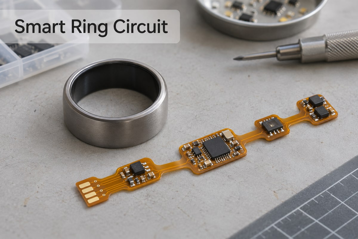
What Does a Smart Ring Circuit Include?
A typical rechargeable smart ring circuit includes sensing devices, a BLE controller, power management, an antenna, and supporting components. The required smart ring functions determine which blocks belong in the design and what must be checked before selecting them.
Use the following checks to identify mismatches before committing to the schematic and PCB layout.
| Circuit Block | Selection Check | Consequence for the Design |
|---|---|---|
| Optical sensor and LEDs | Supply rails, optical window, LED drive requirements | Reserve optical clearance and budget sampling current |
| Motion or temperature sensor | Interface, orientation, thermal path to measurement point | Set placement according to the intended measurement |
| BLE controller | Required interfaces, firmware memory, package pinout | Confirm pin allocation before footprint selection |
| Battery and power management | Cell charge limits, rail voltages, peak load | Match charger settings and regulator capacity |
| Antenna and matching network | Reference layout, keep-out, final housing materials | Reserve tuning access and validate after enclosure assembly |
These blocks do not necessarily require separate chips. A Bluetooth system-on-chip can combine the processor and radio, while a power-management IC can integrate charging and regulation. The bare PCB board provides the interconnections; the assembled board adds the components needed to perform those functions.
How Does Smart Ring Hardware Connect Sensors, BLE, and Power?
Smart ring hardware connects sensors to a controller through digital interfaces, distributes compatible supply rails, and connects the BLE radio to an antenna. A smart ring works by collecting sensor data, processing or buffering it, and transmitting selected information under firmware control.
- Sensor interfaces: Check I²C or SPI support, interface voltages, pull-ups, and interrupt pins together. Selecting a smart ring chip by package size alone can leave too few connections or insufficient memory for the intended firmware.
- Power distribution: Check each device's supply requirements before drawing the power tree. The MAX30101 uses separate supplies for its internal circuitry and LEDs; the BQ25120A integrates charging, a power path, and voltage regulation. These examples illustrate integration choices, but the selected battery and loads still determine compatibility.
- Radio connection: Follow the selected controller's RF reference layout and preserve antenna keep-out space. Include access for matching adjustments, because the final housing and proximity to the finger can affect radio behavior.
- Operating schedule: Budget current across LED pulses, sampling, processing, BLE activity, sleep, and regulator losses. Define how often each function runs before estimating battery life; a chip's sleep-current figure cannot represent the complete ring.
Smart Ring PCB Design: How Does the Board Fit a Curved Housing?
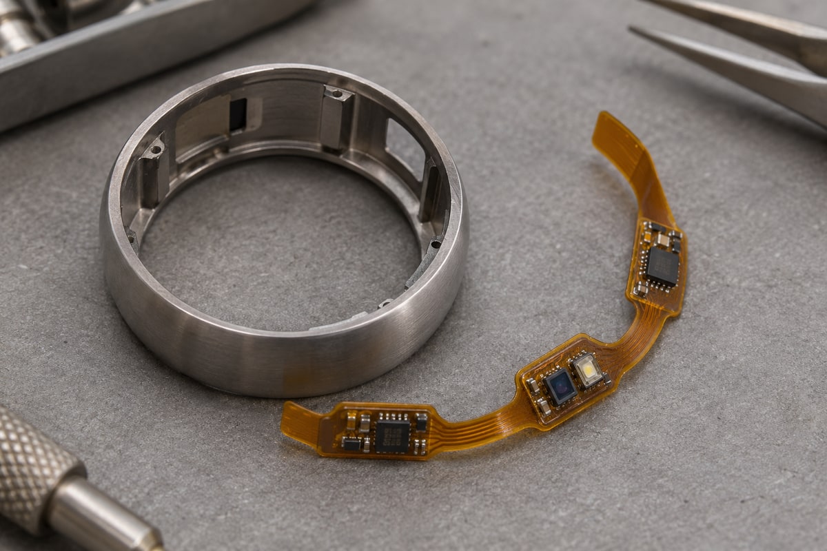
Smart ring PCB design fits the electronics into a curved housing by separating supported component areas from sections that can bend. Check the flat manufacturing layout and the installed shape together before freezing the board outline.
- Choose the support structure: A smart ring circuit board can use flex with local stiffeners or rigid-flex with rigid component islands. Compare component support, routing requirements, and available thickness. Specify stiffeners and rigid sections separately because their constructions differ.
- Build the full thickness stack: Include component heights, coverlay, adhesives, reinforcement, battery clearance, and enclosure tolerances. Check the tightest cross-section rather than relying on nominal bare-board thickness.
- Define the bend zones: Keep component bodies and solder joints out of intended bends. Review trace routing and stiffener-edge transitions with the manufacturer, and state whether the board is formed once or repeatedly flexed during use.
- Locate the optical window and antenna: Confirm sensor-to-window alignment in the formed model and preserve the antenna's required clearance. A flat layout that fits the outline can still place these parts incorrectly after installation.
What Makes a Smart Ring Design Ready for PCB Assembly?
A smart ring design is ready for assembly when its component data, land patterns, panel support, and installation sequence describe a buildable assembly. Small packages alone do not establish production readiness; the factory must be able to print, place, solder, inspect, and handle the board consistently.
- Package and BOM alignment: Match each ordered part to its footprint, pin numbering, polarity, and height limit. Identify approved substitutions before purchasing.
- Pad and coverlay coordination: Check solderable openings and mask or coverlay clearances against the assembly process. Include optical keep-out requirements from the sensor documentation.
- Panel and carrier support: For high-density SMT assembly on FPCs, agree on how the panel will be held flat through printing, placement, and reflow. Define fiducials and handling areas before panel release.
- Post-reflow operations: Specify when to attach the battery, program firmware, form the circuit, and install it in the housing. Confirm the temperature restrictions of parts added after reflow.
Discuss inspection access before components become hidden by the enclosure. This determines whether a defect can be found and repaired at board level or only discovered after further assembly work.
How Should a Smart Ring Circuit Be Tested?
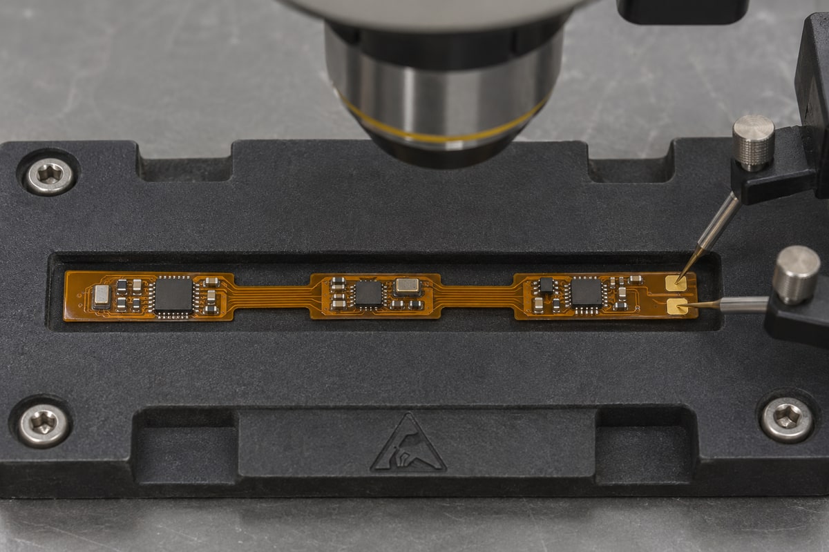
A smart ring circuit should be tested in stages, with separate acceptance criteria for the bare board, assembled electronics, and completed device. This makes failures easier to isolate before additional assembly hides the circuitry or increases rework cost.
- Bare-board electrical checks: Test the specified nets for opens and shorts. Use the released fabrication data as the reference; continuity alone does not validate circuit operation.
- Assembly inspection and first power-up: Inspect placement, polarity, and solder joints, then apply power under controlled conditions. Check supply rails and abnormal current before proceeding to application tests.
- Programmed functional checks: For a programmable smart ring, provide the firmware revision, programming interface, fixture connections, and pass/fail limits. Check sensor communication, charging behavior, operating-mode current, and BLE communication against those limits.
- Completed-device validation: Test optical performance, radio behavior, runtime, and sealing with the actual housing and defined use conditions. Assign these tests to the responsible product team or agreed test provider; they are separate from bare-board and PCBA acceptance.
A sensor returning its identification register confirms communication, not physiological measurement accuracy. Specify which functional outputs the factory must check so that a communication test is not mistaken for complete sensor validation.
What Files Does an Open Source Smart Ring Need for Manufacturing?
An open source smart ring needs a consistent release that defines fabrication, component procurement, assembly, mechanical fit, and testing. A smart ring schematic establishes electrical connections, but it cannot by itself tell a factory how to build and accept the physical product.
When reviewing a smart ring project on GitHub, confirm that the files belong to the same revision and that their licensing permits your intended reuse. Use this table to decide whether the package is ready for a manufacturing review or needs clarification first.
| Release Package | Cross-Check Before Submission | Issue to Resolve Before Build |
|---|---|---|
| Gerbers, drills, stackup, fabrication drawing | Layer order, outline, thickness, stiffener and bend locations agree | Conflicting board construction or missing mechanical definition |
| BOM and schematic | Part numbers, reference designators, fitted quantities agree | Unspecified parts or unapproved substitutions |
| Placement file and assembly drawing | Board origin, units, side, rotation, polarity agree | Ambiguous placement or component orientation |
| Housing model and formed-board drawing | Component heights, battery space, optical opening align | Interference or sensor-window mismatch |
| Firmware and test procedure | Hardware revision, programming access, acceptance limits agree | No reproducible way to program or accept assemblies |
If you are evaluating how to make a smart ring, begin with functional evaluation on development hardware, then move to the custom board, formed assembly, and enclosed-device validation. For each build, issue one identified release and resolve the discrepancies above before production starts.
How Can BestFPC Support Your Smart Ring Project?
We support your smart ring project through board manufacturability review, flex or rigid-flex fabrication, and coordinated sourcing, assembly, and agreed testing in China. Our support connects your released design with the manufacturing steps needed for prototype and small-batch builds.
- Engineering feedback before release: Our technical team can provide a DFM pre-review report and BOM optimization list, highlighting manufacturing conflicts and component options for your engineers to approve. This gives the team specific issues to close before ordering boards and parts.
- Construction matched to the housing: We review adhesive or adhesiveless flex materials, coverlay, and PI reinforcement against your geometry and component-support needs. The aim is to select a buildable construction that fits the assembly, rather than defaulting to the thinnest material.
- Coordinated PCB and PCBA delivery: We integrate PCB fabrication, component procurement, assembly, and the agreed test scope. Define programming responsibilities and acceptance limits during quotation so the delivered assemblies match your next development step.
- Prototype and small-batch support: We support initial builds for design verification and subsequent revisions. Agree on the quantity and revision for each run so engineering changes can be evaluated before committing to a larger order.
FAQs about Smart Ring Circuit
Can a smart ring development kit be used directly for production?
Usually, it is a starting point for evaluating sensors, connectivity, and firmware. Its board shape, power consumption, and interfaces may differ from the final product. Use the kit to validate functions, then verify them again on the custom hardware.
Does every smart ring need a battery?
No. A passive NFC ring can draw energy from a nearby reader for a brief interaction. A ring that continuously samples sensors or communicates actively over BLE generally needs its own power source.
Can an unavailable component be replaced with a similar part?
Only after checking more than the package. Compare pinout, voltage requirements, interface behavior, firmware support, and optical or radio characteristics where relevant. A substitution may require new validation even if no PCB layout change is needed.
Can one board design serve several ring sizes?
Possibly, if the housing and assembly arrangement accommodate it. Check the formed geometry, battery space, antenna position, and optical alignment for every size. Shared electronics do not automatically mean identical mechanical or radio performance.
What should change in the files after a prototype correction?
Update the affected design files and issue a new, identifiable release. Synchronize the BOM, fabrication outputs, placement data, firmware, and test instructions as applicable. Document the change so the factory does not combine corrected files with an older build package.
Bring your circuit, mechanical constraints, and expected delivery scope to BestFPC for a manufacturing review. Our technical team can provide a DFM pre-review report and BOM optimization list, giving your engineers specific manufacturing issues and component options to resolve before release. We combine PCB fabrication, component sourcing, PCBA assembly, and agreed testing in one coordinated workflow, helping reduce handoff gaps between suppliers. Prototype and small-batch support lets you evaluate the compact assembly and incorporate engineering changes before increasing order quantities. Contact sales@bestfpc.com to discuss your project.


.png)
.png)
.png)
.png)

.png)