


 2026-11-09

 BEST
A shielded flex PCB combines a flexible interconnect with a conductive shielding structure to help manage electromagnetic interference. For OEM buyers, the purchasing decision includes the shield material, ground connections, finished thickness and signal requirements—all within the space available for installation or movement.
At BestFPC, we combine custom flexible circuit manufacturing, controlled-impedance capability and assembly support for OEM projects. The United States, Germany and Israel were our largest export markets by volume last year, reflecting our experience serving international buyers. Our team reviews shielding, stackups and connector support against your requirements. Send your drawings and quantities to sales@bestfpc.com to discuss fabrication and assembly options.
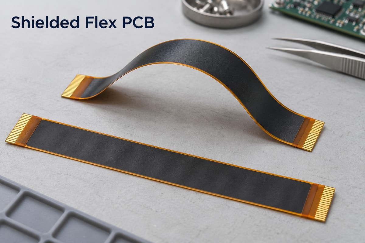
Top 10 flex pcb manufacturers emi shielding high-reliability
BestFPC, All Flex Solutions, Epec, Minco, PICA, PFC, Flexible Circuit Technologies, Sierra Circuits, Rush PCB and I-Tech are ten suppliers to consider when sourcing flex circuits with EMI shielding. This comparison highlights relevant capabilities rather than assigning an industry ranking.
| Manufacturer | Manufacturing Capabilities | Core Strength / Positioning |
|---|---|---|
| BestFPC | Standard 1–4-layer FPC; ±10% impedance; 0201 assembly | Engineering-led FPC fabrication and turnkey assembly |
| All Flex Solutions | Up to 8-layer flex; unbonded regions; EMI/RFI shielding | Multilayer flex with controlled impedance and shielding |
| Epec Engineered Technologies | Up to 20-layer flex; 0.003-inch lines; film/copper/ink shielding | Complex flex and rigid-flex interconnects |
| Minco | Rigid-flex assembly; 0201 SMT; integrated copper shields | Engineered interconnect assemblies for demanding applications |
| PICA Manufacturing Solutions | 50 µm rigid-flex traces/spaces; TDR impedance verification | Flex/rigid-flex engineering and broader assembly integration |
| PFC Flexible Circuits | 50 µm lines/spaces; up to 16-layer rigid-flex | Flex design, fabrication and assembly under one roof |
| Flexible Circuit Technologies | Etched copper, conductive-ink and laminated-film shielding | Custom flex through assembled products and box builds |
| Sierra Circuits | Up to 12-layer flex; 16-layer rigid-flex | Flex/rigid-flex and HDI fabrication with NPI support |
| Rush PCB | EMI-shielded 2-layer polyimide flex; PCB assembly | Prototype fabrication and assembly across PCB types |
| I-Tech | Silver/copper-type films; 0.5 × 0.5 mm ground windows | Shielded-FPC lamination and grounding-process integration |
Layer counts and feature sizes describe different product families and process conditions; confirm the complete shielded stackup with each supplier. Rush PCB’s two-layer entry is a published product example, not its maximum layer capability.
For high-reliability applications, ask flex PCB manufacturers how EMI shielding will be specified and verified on your actual construction. A useful quotation identifies the proposed material, grounding arrangement, impedance acceptance criteria and any required mechanical validation. Compare those commitments alongside price; the word “shielded” alone does not define the deliverable.
Shielded Flex PCB Products BestFPC Manufactures
We manufacture custom shielded flexible circuits with defined shield coverage, connection areas and local reinforcement. Product selection starts with the interconnect you need to install, then adds the electrical and mechanical requirements for that route.
- Shielded flex interconnects: Flexible tails connecting separate boards or modules, with exposed contacts or solderable terminals kept accessible. These structures can suit display, camera and sensor connections in compact equipment.
- Double-sided and multilayer flex: Additional routing and reference layers for designs that need more than a simple signal tail. Shield coverage is coordinated with the copper structure and available thickness.
- Shielded rigid-flex constructions: Flexible links between rigid component areas where the product needs both a routed interconnect and stable mounting regions. The flex-to-rigid transition and shield termination require separate drawing details.
- Locally reinforced flex: PI or other approved stiffeners at connection and assembly areas, while the intended flexing region remains clear of unnecessary reinforcement.
Specify whether your shielded flexible circuit bends only during installation or moves repeatedly in service. That distinction affects the construction we evaluate, particularly the placement of stiffener edges, ground contacts and shield boundaries.
Our Shielded Flex PCB Manufacturing Capabilities
Our FPC manufacturing options include adhesive-based and adhesiveless polyimide constructions, local stiffeners and controlled impedance. The following standard FPC parameters provide a starting point for reviewing a shielded design.
| Manufacturing parameter | Standard FPC capability |
|---|---|
| Circuit layer count | 1–4 layers |
| Finished board thickness | 0.06–0.60 mm |
| Base construction | Adhesive-based or adhesiveless PI |
| PI stiffener thickness | 3, 5, 7 or 9 mil |
| Controlled-impedance tolerance | ±10% |
These are individual FPC capability ranges, not a guarantee that every combination is available. The quoted shielded stackup must account for the shield, adhesive, coverlay and any local reinforcement; impedance tolerance applies to an agreed target, construction and measurement arrangement.
For example, a thin flex tail and a reinforced connector end have different thickness requirements. Giving each region its own dimension helps prevent the connector specification from being incorrectly applied across the flexible span.
Custom EMI Shielding Film and Impedance Control Solutions
We assess EMI shielding film together with the signal stackup, ground access and bending requirements. This lets the shield become part of the manufacturing specification before material selection and tooling are finalized.
Our EMI shielding design review addresses three connected requirements:
- Thin construction: Select EMI shielding film for flexible electronics by its laminated thickness, adhesive system and suitability for the required movement. For electronic devices with limited space, the relevant dimension is the complete finished flex stack, including the protective layers.
- Ground connection: Define coverlay openings over the intended ground copper, with sufficient contact area and registration allowance. An EMI shield film needs a specified electrical connection; ordinary insulating coverlay does not provide that connection by itself.
- Signal performance: Include the shield and its spacing from the traces in the impedance assessment. Maintain the intended copper reference structure unless the alternative has been evaluated electrically; a shielding film should not automatically replace a high-speed return plane.
When selecting flexible EMI shielding materials for electronics, compare the construction change as well as the material. Common PCB shielding techniques include copper planes, laminated films and printed conductive coatings. Copper can provide a defined reference structure but adds stiffness; films can suit thin constructions; conductive coatings require evaluation of their conductivity, thickness and mechanical behavior. The appropriate EMI shielding techniques depend on the complete circuit and the supplier's available process.
Effective PCB EMI shielding design also separates three product categories: the shielding layer, the conductive bonding or grounding materials, and any connector or enclosure contacts. These parts work together to address EMI grounding and shielding on flexible printed cables, but they are not interchangeable.
For flex PCB manufacturing with EMI shielding and impedance control, send the target impedance, critical nets, intended reference layers and shield outline together. Planning EMI shielding in flex PCB design at this stage avoids approving a signal stackup that must later change to accommodate the shield.
Shielded Flex PCB Assembly Services
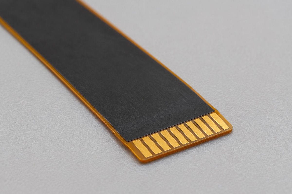
We support flex PCB assembly alongside bare-board manufacturing, including component sourcing, SMT placement and connector installation. The assembly plan considers the shield surface, reinforced mounting areas and access to solder joints.
Available assembly support includes:
- Component procurement: Full turnkey, partial turnkey or consigned components, with BOM and approved-part information defining purchasing responsibility.
- SMT placement: Capability includes 0201 packages, subject to the actual layout and flex support. General equipment limits include components up to 45 × 45 mm and placement height up to 15 mm; suitability still depends on the individual assembly.
- Flex handling: Carriers and fixtures support thin circuits during printing, placement and reflow. Component areas need adequate local support without transferring strain into the moving tail.
- Assembly inspection: First-article inspection, SPI, AOI and X-ray capabilities can be selected for the build. ICT or functional testing requires an agreed test scope and suitable access or fixtures.
Keep shield contacts, exposed pads and connector mating areas clearly identified in the assembly drawing. This helps coordinate the lamination and assembly sequence without covering a required connection or obstructing inspection.
Quality Control for Shielded Flexible Circuit Production
Our quality process includes incoming-material checks, in-process inspection and electrical testing before shipment. For shielded flexible circuit production, the acceptance plan must also define which shield-related features need inspection or measurement.
A shielded-board acceptance plan should address:
- Geometry and appearance: Outline, contact dimensions, local thickness, shield coverage and visible lamination defects.
- Electrical connectivity: Circuit continuity and isolation, plus the specified connections between the shield and ground. Shield contact resistance needs a defined limit and measurement method if it is an acceptance requirement.
- Controlled impedance: The agreed target, tolerance, test structure and reporting arrangement for the critical nets.
- Mechanical validation: Installation bend or repeated-motion conditions, including the radius, movement and acceptance criteria when such testing is required.
A material supplier's shielding-effectiveness value describes a particular test setup. Finished-board shielding performance also depends on coverage, grounding and frequency, so a specific attenuation requirement needs an agreed test method for the relevant construction.
Shielded Flex PCB Prototypes and Production Orders
We support prototypes, small batches and production orders, helping your engineering team move from initial fit checks to a repeatable manufacturing specification.
- Prototype builds: Produce the initial construction for connector-fit, routing and electrical evaluation. Identify which shield materials, dimensions and grounding details are fixed and which can be adjusted after evaluation.
- Small-batch validation: Apply approved prototype changes to a pilot build before increasing quantities. Where assembly is included, align the BOM, placement data and inspection requirements with the updated board revision.
- Production release: Bring the fabrication drawing, stackup, shield artwork and assembly files to one approved revision. Freeze the material specification and acceptance criteria so repeat orders use the same baseline.
- Repeat orders and changes: Reference the released package when reordering. Review material substitutions or design changes for their effects on thickness, grounding and impedance before approval.
Shielded Flex PCB Cost and Lead Time
Shielded flex PCB pricing combines bare-circuit fabrication, shielding operations and the selected inspection or assembly scope. We quote lead time against the approved files, material availability and order quantity, with production and shipping timing identified separately for US buyers.
The main quotation variables are:
- Circuit geometry: Layer count, outline and panel utilization influence material use and processing cost. A long or irregular tail may use a panel less efficiently than a compact outline.
- Shield construction: Film grade, coverage on one or both faces, grounding details and additional lamination operations affect the build.
- Order quantity: Tooling and setup charges can have a larger effect on prototype unit cost. Request separate non-recurring and recurring charges when comparing quantities.
- Delivery scope: Bare boards, assembled circuits, special inspection records and application-specific fixtures are different deliverables and should be priced accordingly.
A specified film with a procurement lead time can govern the schedule even when the circuit itself is straightforward. For a useful comparison, ask for quotes against the same material specification, acceptance requirements and delivery basis.
Case Study: Shielded Flex PCB for a USB 2.0 Interconnect
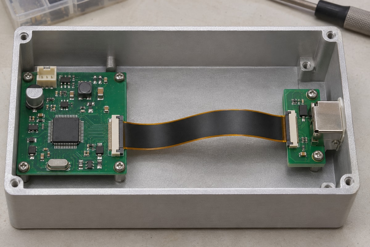
Application: This two-layer shielded FPC suits an internal USB 2.0 link in a compact test instrument, connecting the controller board to a housing-mounted interface for measurement-data transfer to a computer. It carries D+/D− signals, power and ground, with a separate shield connection.
Manufacturing Challenges:
- Limited Routing Space: The interconnect must fit between the controller board and interface connector without making the contact end too thick for insertion.
- Shield and Signal Coordination: Shielding on both faces must work with the impedance-controlled signal structure while retaining the specified separation between shield and circuit ground.
- Localized Connector Support: The gold-finger end needs reinforcement, while the connecting span must remain flexible for installation.
BestFPC Manufacturing Solutions:
- Region-Specific Thickness Control: We review the flex stackup and reinforced contact end as separate dimensions, matching the connecting span to the installation space and the terminal area to the mating connector.
- Coordinated Shielding and Impedance Review: We evaluate the shielding layers alongside the D+/D− routing and reference structure. The fabrication artwork must preserve the dedicated shield contact rather than automatically connect it to the signal-ground net.
- Local PI Reinforcement: The specified PI stiffener supports the gold-finger area. Its boundary follows the connector-support requirement so reinforcement does not unnecessarily extend into the installation bend.
Customer Benefits: This construction gives equipment designers a thin internal USB interconnect with a supported contact end and a defined shield path. Reviewing these features together helps resolve connector fit, installation clearance and electrical connection requirements before prototype release.
PCB Specifications:
| Product Parameter | Specified Construction |
|---|---|
| Circuit layers | 2 |
| Copper | 1 oz rolled-annealed copper |
| PI base / coverlay | 1 mil / 1 mil |
| Flex thickness | 0.23 ± 0.03 mm |
| Reinforced contact-end thickness | 0.33 ± 0.03 mm |
| Shield coverage | Both faces |
| Surface finish | ENIG; 1 µin gold |
Why Choose BestFPC as Your Shielded Flex PCB Manufacturer?
BestFPC combines quality management credentials, experienced engineering support and integrated manufacturing services for shielded flex PCB projects. We help your team resolve fabrication and assembly requirements before production begins.
- Quality management certifications: Our credentials include ISO 9001, ISO 13485, IATF 16949 and AS9100D. These quality management systems support supplier qualification and structured control of manufacturing processes, giving procurement teams a basis for evaluating quality requirements for their projects.
- Experienced engineering and DFM support: Our R&D and PCB/PCBA engineers bring 20 years of experience to DFM analysis and process recommendations. We provide DFM pre-review reports and BOM optimization lists, helping your team address shield grounding, impedance stackups, connector reinforcement and component choices before releasing the build.
- One-stop fabrication and assembly: We integrate PCB manufacturing, component sourcing, PCBA assembly and testing. For shielded flex projects, this connects the shield construction and stiffener layout with component placement, assembly fixtures and inspection requirements, reducing handoffs between separate suppliers.
Our FPC fabrication and shielding support focuses on delivering the agreed circuit construction. Share the operating constraints with the drawing so we can identify manufacturing questions before they become production changes.
FAQs about Shielded Flex PCB
Can BestFPC quote from existing Gerber files?
Yes. Send the Gerber files with a fabrication drawing, quantities and shield requirements. If the shield outline or material is missing, identify that item as open for review so the quotation can state its assumptions clearly.
What bending information should accompany an inquiry?
Provide the bend location, minimum installed radius and whether movement occurs once or repeatedly. For repeated motion, include the movement pattern, expected cycles and operating conditions so construction and validation requirements can be discussed together.
Can bare boards and assembled circuits be quoted separately?
Yes. Request separate fabrication and assembly pricing, and include the BOM and placement data for the assembly option. State whether you will supply components or need us to purchase them.
Can a different shielding film be used if the specified grade is unavailable?
An alternative requires customer approval. Compare the laminated thickness, adhesive and grounding behavior, electrical characteristics and relevant mechanical requirements before accepting the change.
Will an engineering change affect a repeat-order quotation?
It can. Changes to the outline, layer structure, shield artwork or assembly may require revised tooling, materials or inspection arrangements. Submit the new revision and a change summary for assessment before placing the repeat order.
Does a shielded board guarantee a pass in FCC EMI testing?
No. A shielded board is one part of the electronic system. Enclosure openings, other cables, connectors and operating modes also influence emissions, so finished-product testing must address the complete assembly.
At BestFPC, PCB/PCBA engineers with 20 years of experience provide DFM pre-review reports and process recommendations for shielding, impedance and connector-support requirements. We integrate PCB manufacturing, component sourcing, turnkey PCBA assembly and testing, supporting prototypes and small batches through production. For a shielded flex PCB quotation, send your Gerber files, stackup, shield outline, target impedance and quantities to sales@bestfpc.com, together with the BOM if assembly is required. Our team can then assess the manufacturing scope and delivery requirements for your project.


.png)
.png)
.png)
.png)

.png)