


 2026-11-19

 BEST
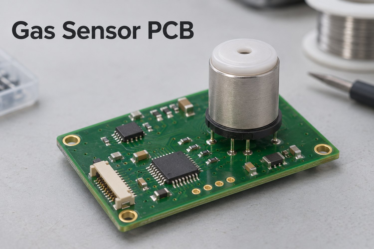
A Gas Sensor PCB supports the sensing element, its power supply, and the circuitry that carries or processes its output. Depending on the product, it may be a simple carrier board, an assembled sensor interface, or part of a larger gas detector. The sensor technology determines the electrical and assembly requirements.
At BestFPC, we combine PCB manufacturing, component sourcing, and PCBA assembly with DFM support for compact gas detection products. Our PCB and PCBA engineers review your board structure, sensor footprint, and assembly requirements before production. With prototype and small-batch support, we help you move from approved drawings to a build ready for evaluation. Send your requirements to sales@bestfpc.com.
What Gas Sensor PCB Solutions Does BestFPC Provide?
BestFPC provides custom bare boards and PCB assemblies for gas sensing products, with the supply scope defined by your fabrication files and BOM. We support rigid, flexible, and rigid-flex constructions according to the mounting arrangement and available enclosure space.
- Sensor carrier boards: A gas sensor board can connect the sensing element to headers, sockets, or a host board without including the complete detection electronics.
- Assembled interface boards: A gas sensor module circuit may include an analog front end, power components, signal conditioning, and connectors. We manufacture and assemble the approved circuit rather than treating every sensor interface as the same design.
- Flexible interconnections: FPC tails can connect a sensor head to a separate controller or display. Component and connector areas need suitable support; the flexible section accommodates the installation geometry.
- Integrated rigid-flex boards: Rigid areas support components while flexible sections link separated circuit areas inside the housing.
For an LPG gas sensor circuit, heater power and the sensor's specified operating cycle can affect the assembly and test plan. A VOC monitoring board may instead use a digital sensor with its own processing requirements. These are different builds, even when both are described as gas detection boards.
Gas Sensor Board Manufacturing Capabilities
Our gas sensor board manufacturing capabilities cover thin polyimide circuits and rigid-flex structures for compact sensor assemblies. The following parameters help establish a manufacturable starting point before we review the complete stackup.
| Manufacturing Parameter | Capability |
|---|---|
| Flexible circuit layer count | 1–4 layers |
| Finished flexible board thickness | 0.06–0.60 mm |
| Rigid-flex layer count | 2–20 layers |
| Rigid-flex board thickness | 0.3–3.0 mm |
| Rigid-flex inner trace/space, 18 μm copper | 3/3 mil (76.2/76.2 μm) |
| Rigid-flex inner trace/space, 35 μm copper | 4/4 mil (101.6/101.6 μm) |
| FPC outer trace/space, 18 μm copper | 3.5/3.5 mil (88.9/88.9 μm) |
| FPC outer trace/space, 35 μm copper | 4/4 mil (101.6/101.6 μm) |
| PI stiffener thickness options | 3, 5, 7, 9 mil |
| FPC surface finish options | ENIG, plated gold, OSP, tin plating |
Trace/space values are before compensation and refer to the stated finished copper thickness. Board thickness and layer-count limits require stackup review; rigid and flex regions are specified separately.
For layout review, increasing the specified copper thickness from 18 μm to 35 μm changes the listed rigid-flex inner trace/space from 76.2/76.2 μm to 101.6/101.6 μm. A fine-pitch escape route therefore needs to be checked against both copper thickness and layer location before release.
We can use adhesive or adhesiveless polyimide constructions as appropriate. For a connector tail, a 5 mil PI stiffener equals 0.127 mm, but that is only the stiffener: the mating thickness must also include the circuit, coverlay, and adhesive.
How Is a Gas Sensor Breakout Board Matched to the Sensor Package?
A gas sensor breakout board must match the exact sensor's land pattern or lead arrangement, mechanical envelope, and gas-access requirements. A similar package outline does not establish pin compatibility.
For example, the Sensirion SGP40 measures 2.44 × 2.44 × 0.85 mm, uses an I²C interface, and operates from 1.7–3.6 V. These figures let the team check package height, supply compatibility, and host connections. The body dimensions alone are insufficient to create its PCB footprint.
Our footprint review checks four interfaces:
- Electrical: Verify pin numbering, sensing electrodes, heater terminals, and any unused connections against the selected part number.
- Soldering: Match pad geometry, drill and finished-hole requirements, solder-mask openings, and the manufacturer's permitted soldering method.
- Mechanical: Check sensor height, mounting support, connector orientation, and clearance to the enclosure. A large sensor body should not rely on an unsupported flexible section for mechanical support.
- Gas access: Keep the sensing opening clear of adhesive, coating, mounting hardware, and housing features that could obstruct exposure.
When specifying a gas sensor for PCB mounting, supply the manufacturer's package drawing and assembly instructions with the BOM. This lets us assess the footprint against the actual component rather than a generic library name.
How Does BestFPC Support Electrochemical Gas Sensor Circuit Assembly?
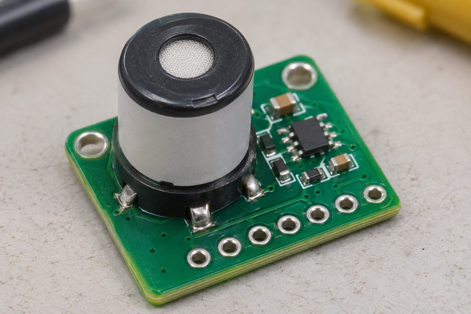
We support electrochemical gas sensor circuit assembly by reviewing the approved board and BOM for manufacturability, component placement, cleanliness, and test access. The sensing interface must suit the cell's electrode configuration and bias requirements.
A component-level example is the TI LMP91000, which supports 2.7–5.25 V operation and seven programmable transimpedance gains from 2.75 kΩ to 350 kΩ. The selected gain and reference settings belong in the build and test instructions; fitting the correct IC does not confirm that its operating configuration is correct.
The assembly review focuses on:
- Low-current signal paths: Identify sensitive input nodes and keep the specified clearances and guard features intact. Residue or unintended leakage can interfere with small sensor currents.
- AFE components: Verify the approved amplifier or potentiostat, feedback components, and their placement. A threshold comparator does not replace a complete electrochemical sensor interface.
- Power and switching sections: Review the physical separation of sensitive circuitry from switching supplies, alarm drivers, and other disturbance sources. Circuit performance remains subject to the customer's design validation.
- Cell installation: Follow the selected sensor's handling, connection, and thermal limits. Use sockets or a separate installation operation when required by its instructions.
- Test access: Provide accessible supply and output connections so the agreed fixture can check the board without damaging the sensor connection.
For a gas detector sensor circuit, our DFM findings identify fabrication or assembly issues for approval before release. Changes to sensor bias, analog gain, firmware, or alarm thresholds require approval from the product's design owner.
How Is Sensor Contamination Controlled During Gas Sensor PCB Assembly?
Contamination control starts with the selected sensor's handling instructions and a compatible assembly sequence. Cleaning, conformal coating, adhesive curing, and packaging must be assessed for their effect on the exposed sensing element.
The production plan should define:
- Cleaning restrictions: Identify whether the fitted sensor permits board washing or solvent exposure. If it does not, evaluate cleaning before sensor installation or an approved process that avoids washing the assembled sensor.
- Flux selection: Specify a suitable soldering process and residue requirements. A no-clean flux designation alone does not establish compatibility with a sensitive gas sensor.
- Coating boundaries: Mark areas that must remain uncoated, including the gas opening and any restricted package surfaces. Coating the whole board indiscriminately can prevent the sensor from working correctly.
- Adhesive and housing materials: Check for substances that may outgas near the sensor, especially where adhesive, potting material, or seals are used close to the air path.
- Handling and packing: Protect the sensing surface from contact, debris, and unsuitable packaging materials while maintaining the required ESD precautions.
The electrical impact can be quantified with an illustrative calculation: 1 V across a 1 GΩ leakage path produces 1 nA. If that current enters a node carrying a 100 nA sensor signal, it equals 1% of the signal. These are assumed circuit values, not measured board results; they show why residue and leakage control matter even when the board looks clean.
How Is a Gas Detector PCB Tested Before Delivery?
A gas detector PCB is checked against the agreed bare-board and assembly acceptance criteria. Electrical connectivity, solder-joint inspection, and circuit function require different checks; gas response and calibration need a separately defined procedure.
| Test Stage | Check | Acceptance Basis |
|---|---|---|
| Bare-board electrical test | Opens and shorts | Approved netlist |
| Assembly inspection | Placement, polarity, solder joints | BOM and assembly criteria |
| X-ray, where applicable | Hidden solder connections | Package-specific acceptance criteria |
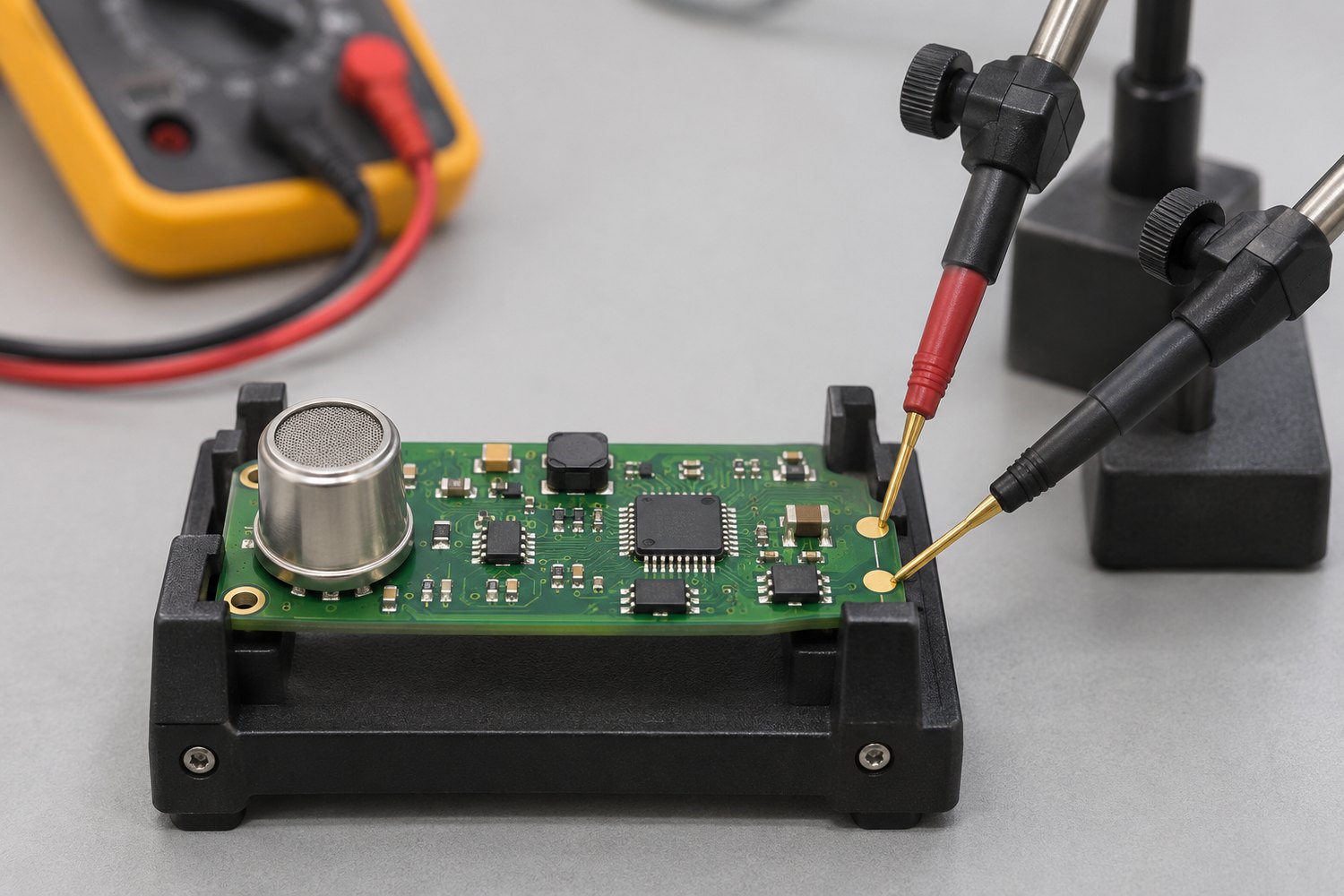
| Powered functional test | Rails, outputs, communications | Approved fixture and test limits |
| Gas-response calibration | Response to specified gas conditions | Separately agreed gas-test procedure |
For an illustrative current-input test at a nominal 350 kΩ transimpedance gain, inputs of 0, 50, and 100 nA correspond to ideal output-change magnitudes of 0, 17.5, and 35 mV, respectively. This calculation uses ΔV = I × R, assumes linear operation with sufficient output headroom, and excludes offset and gain errors. Actual acceptance limits must include circuit and fixture tolerances.
This kind of signal injection checks the electrical path; it does not establish gas sensitivity, response time, or cross-sensitivity.
For a gas detector circuit with an alarm output, the test specification should state the input condition, expected output, and pass/fail limit. Product certification and hazardous-location approval are separate from PCB fabrication and routine PCBA inspection.
How Long Does Gas Sensor PCB Production Take?
Our fast-turn PCBA service can support approximately 1.5 weeks when materials are available, manufacturing files are approved, and the required processes and tests fit the agreed schedule. The confirmed delivery date depends on the complete build; this timeframe is not a blanket lead time for every bare board or assembled detector.
To establish the production schedule, provide:
- Manufacturing files: Gerber or ODB++ data, stackup, fabrication drawing, and assembly drawing.
- Component information: BOM with manufacturer part numbers, approved alternatives, and customer-supplied parts clearly identified.
- Sensor requirements: Handling restrictions, installation method, and any required stabilization or conditioning period.
- Acceptance requirements: Firmware, programming instructions, fixtures, and functional-test limits where applicable.
We confirm component availability and any fixture preparation before committing to the shipment date. Sensor conditioning or gas-response testing, when included, must be scheduled explicitly rather than absorbed into an assumed standard assembly cycle.
Gas Sensor Board Case Study: Portable Gas Detection
Application
A compact portable detector may need its sensor head positioned near the housing's gas inlet while the controller sits elsewhere inside the enclosure. A four-layer rigid-flex sensor-board construction supports this arrangement: rigid sections carry components, and a flexible section connects the separated areas. The application example below uses a sensor-board construction from our manufacturing records; it illustrates a possible layout for portable gas detection.
Manufacturing Challenges
- Separate thickness windows: The specified 0.8 ± 0.1 mm overall thickness allows 0.70–0.90 mm, while the 0.14 ± 0.03 mm flex section allows 0.11–0.17 mm. Housing and support features must accommodate these ranges.
- The flex transition must accommodate installation without concentrating stress at the rigid edge or nearby solder joints.
- The panel arrangement must support fabrication and assembly while preserving the finished board outline.
BestFPC Manufacturing Solutions
- Define separate inspection limits for the rigid and flex regions. Check enclosure fit against the 0.90 mm overall upper limit and flex routing against the 0.17 mm flex upper limit, rather than using nominal thickness alone.
- Keep component joints and unsupported terminations outside the intended bending region; review the transition against the installation drawing.
- Confirm the production panel and stackup with the customer before release, with shipment inspection documentation included in the build requirements.
Customer Benefits
This construction gives the product designer a way to position the sensing area independently of the main electronics while retaining rigid support for mounted components. Its thin interconnection section accommodates enclosure geometry without requiring the complete circuit board to occupy one plane.
PCB Specifications
| Parameter | Specification |
|---|---|
| Construction | Four-layer rigid-flex |
| Board dimensions | 77.40 × 39.54 mm |
| Base materials | FR4 Tg130 / polyimide |
| Copper weight | 1 oz |
| Flex polyimide core | 0.5 mil (12.7 μm), adhesiveless |
| Overall board thickness | 0.8 ± 0.1 mm |
| Flexible section thickness | 0.14 ± 0.03 mm |
| Surface finish | ENIG, 1 μin gold |
| Solder mask / legend | Green / white |
Why Choose BestFPC for Gas Detector PCB Manufacturing?
BestFPC combines engineering review, board fabrication, component sourcing, and assembly so that manufacturing decisions can be coordinated across the build. For gas detection products, this helps keep the sensor requirements connected to the PCB and assembly instructions.
- Engineering deliverables: Our PCB/PCBA team and R&D engineers with 20 years of experience provide DFM pre-review reports and BOM optimization recommendations, giving you specific issues to resolve before production.
- Quality systems: Our quality-system portfolio includes ISO 9001, ISO 13485, IATF 16949, and AS9100D. The applicable certification scope should match the manufacturing arrangement; these systems do not certify the finished gas detector.
- Manufacturing and sourcing coordination: Our PCB and PCBA factories, supported by more than 1,000 supply-chain partners, help coordinate board production and component procurement around the approved BOM.
- Prototype and small-batch support: You can evaluate the mechanical fit and assembly before releasing a larger production run.
- Production traceability: Our digital production system supports material and product-batch lookup within 5 seconds, helping the team retrieve the relevant production records when investigating a build issue or checking a revision.
FAQs about Gas Sensor PCB
Does a gas sensor PCB detect gas without a sensing element?
No. The bare PCB provides conductors and mounting features. A working gas sensor circuit also needs the appropriate sensing element, power, and signal-processing or readout components.
Can the same board detect different gases?
Sometimes, but a different sensor may require changes to the footprint, bias, heater operation, analog range, or firmware. Confirm each sensor variant against the approved design rather than substituting it solely because it fits the board.
Can a gas leak detector circuit measure an exact gas concentration?
Only if the selected sensor and complete measurement system support that measurement and are calibrated accordingly. A simple threshold alarm output indicates a switching condition; it is not automatically a calibrated concentration reading.
Can one sensor be used for both LPG leakage detection and VOC monitoring?
A sensor may respond to several gases, but response alone does not establish selectivity or measurement accuracy. An LPG gas leakage detector circuit and a VOC monitoring circuit need separate performance requirements and validation for their intended use.
Is a flexible PCB required for a compact gas detector?
No. A rigid board can suit a flat assembly. Flexible or rigid-flex construction becomes useful when the sensor, controller, or display must occupy different positions or planes inside the enclosure.
Can BestFPC assemble customer-specified sensors?
We review customer-specified or customer-supplied sensors against the BOM, package information, and handling instructions. Identify any storage, soldering, washing, or installation restrictions when requesting the build.
For your next gas sensing project, BestFPC offers DFM pre-review, coordinated PCB and PCBA manufacturing, and prototype support to help resolve assembly requirements before production. Send your drawings, BOM, and sensor requirements for a manufacturing review, or contact sales@bestfpc.com to discuss the required build and test scope.


.png)
.png)
.png)
.png)

.png)