


 2026-11-19

 BEST
A long flexible PCB provides continuous electrical connections across industrial automation systems, medical equipment, aerospace electronics, and other applications requiring extended circuit lengths. Compared with standard-length flexible PCBs, it can reduce intermediate connectors between distributed electronic modules. However, longer circuits demand tighter control over conductor resistance, dimensional accuracy, bending performance, and connection reliability.
Are board-length limitations, excessive connectors, poor mechanical fit, or unreliable electrical connections holding back your project? BestFPC provides custom long flexible PCB manufacturing with extended lengths, special outlines, and customized connector tails. Our free DFM check helps identify potential fabrication and assembly issues before production, reducing unnecessary design revisions and rework.
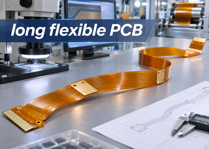
What Is a Long Flexible PCB and Where Is It Used?
A long flexible PCB is an extended-length flexible printed circuit designed to connect electronic components over greater distances. Its length, width, circuit layout, and connection points can be customized to accommodate narrow spaces, distributed electronic modules, and complex equipment structures.
Common applications include:
-
Industrial Automation: Connecting sensors, monitoring modules, and control units distributed along production machinery and automated equipment.
-
Medical Equipment: Providing extended signal connections within diagnostic instruments, medical imaging systems, and patient monitoring devices.
-
Aerospace Electronics: Supporting lightweight interconnections between electronic modules where installation space and weight are restricted.
-
Automotive Electronics: Connecting instrument panels, displays, and distributed electronic components within irregular vehicle structures.
-
Industrial Inspection Equipment: Linking multiple measurement points, inspection modules, and control units across extended equipment structures.
For equipment with widely separated electronic modules, long flexible PCBs can incorporate continuous traces, multiple connector tails, and custom branches to accommodate specific installation requirements.
What Are the Advantages of Long Flexible PCBs Compared to Standard Flexible PCBs?
The main advantage of a long flexible PCB is continuous electrical routing over extended distances, reducing the need for intermediate connections between multiple shorter flexible circuits. This construction can simplify installation and eliminate certain connector-related failure points in larger electronic systems.
| Comparison | Long Flexible PCB | Standard Flexible PCB |
|---|---|---|
| Circuit length | Supports extended continuous routing | Typically used for shorter connections |
| Intermediate connections | Can reduce board-to-board connectors | Longer routes may require multiple boards |
| Installation | Suitable for elongated and complex equipment structures | Better suited to compact electronic assemblies |
| Assembly | May reduce connector installation and joining operations | Convenient for localized module connections |
| Manufacturing | Requires tighter control of extended-length dimensions and registration | Generally compatible with conventional processing dimensions |
Replacing several interconnected flexible boards with one continuous circuit may eliminate contact interfaces susceptible to loosening, poor contact, or assembly errors.
However, greater length does not automatically improve electrical performance or bending life. The benefits depend on circuit construction, conductor dimensions, materials, and operating conditions.
What Length and Size Limitations Apply to Long Flexible PCBs?
The maximum manufacturable length of a long flexible PCB depends on board width, layer count, material dimensions, and processing equipment. Long, narrow single-layer circuits are generally easier to manufacture at extended lengths than wide or multilayer constructions.
The main limitations include:
-
Laminate Dimensions: Polyimide copper-clad laminates and copper foils must accommodate the required processing length. Special dimensions may be restricted by available material formats.
-
Board Width and Length: Increasing circuit width can reduce the maximum available processing length because of equipment limitations.
-
Layer Count: Double-sided and multilayer circuits require additional alignment, lamination, and hole-processing operations, increasing manufacturing complexity.
-
Processing Equipment: Imaging, lamination, drilling, profiling, and electrical testing equipment must accommodate the finished circuit dimensions.
-
Outline Complexity: Multiple branches, irregular profiles, and precision connector tails can complicate material registration and final profiling.
-
Installation Tolerances: Connector positions and intermediate mounting points must align with the equipment structure, particularly when several locations are mechanically fixed.
For circuits installed along curved equipment paths, the developed circuit length should account for the actual routing path, connector positions, and required assembly allowances.
What Materials and Stackups Are Suitable for Long Flexible PCBs?
Polyimide (PI) copper-clad laminate is a common choice for long flexible PCB manufacturing because it provides thermal stability, electrical insulation, and mechanical flexibility. Copper type, protective insulation, and layer construction should match the operating temperature, current requirements, and bending conditions.
Common material options include:
-
Polyimide (PI): Provides thermal stability, electrical insulation, and flexibility for industrial and precision electronic applications.
-
Rolled-Annealed (RA) Copper: Often preferred for repeated-bending applications because of its favorable bending fatigue characteristics.
-
Electrodeposited (ED) Copper: Suitable for many static installations or circuits with limited bending requirements, depending on the specified construction.
-
Adhesiveless Laminates: Reduce adhesive content within the base laminate and can help minimize flexible-area thickness.
-
PI Coverlay: Protects copper traces while leaving specified solder pads and electrical contacts exposed.
Common stackup configurations include:
-
Single-Layer Flexible PCB: A relatively simple, thin construction suitable for extended connections with limited routing requirements.
-
Double-Layer Flexible PCB: Provides additional routing space and can accommodate separate signal and return paths where necessary.
-
Multilayer Flexible PCB: Supports more complex electrical requirements but increases circuit thickness, bending stiffness, and manufacturing complexity.
For dynamic bending applications, thinner flexible constructions with fewer copper layers are generally preferable. Unnecessary copper and insulating layers should be avoided in frequently flexed regions.
How Should Long Flexible PCBs Be Designed for Reliable Electrical and Mechanical Connections?
Long flexible PCB design should prioritize conductor resistance, bending radius, copper routing, signal integrity, and connector geometry. These parameters directly affect electrical performance, mechanical durability, and connection stability over extended distances.
1. Trace Width, Copper Thickness, and Voltage Drop
Conductor resistance increases with circuit length, potentially causing excessive voltage drop and heat generation. Trace width and copper thickness should be selected according to actual conductor length, operating current, allowable voltage drop, and temperature-rise requirements.
-
Trace Width: Wider traces reduce electrical resistance but require more routing space.
-
Copper Thickness: Thicker copper reduces resistance but increases bending stiffness.
-
Supply and Return Paths: Calculate resistance across the complete current loop rather than considering only the outgoing conductor.
-
Operating Temperature: Copper resistance increases with temperature, so voltage-drop calculations should account for actual operating conditions.
For long flexible PCB power connections, establish the allowable voltage drop before determining conductor width and copper thickness.
2. Bending Radius and Flexing Cycles
A flexible circuit bent once during installation has different requirements from a circuit that moves repeatedly during operation. Dynamic applications generally require more careful control of copper type, flexible-area thickness, and bending radius.
-
Static Bending: For preliminary evaluation, single- and double-layer circuits may use a bend radius of approximately 10 times the finished flexible-area thickness or greater. Multilayer structures generally require larger radii.
-
Dynamic Bending: Repeated-motion applications typically require substantially larger bend radii and qualification against the intended number of bending cycles.
-
Material Selection: RA copper and thinner constructions are often more suitable for repeated bending, subject to the actual mechanical conditions.
The allowable bending radius depends on copper thickness, dielectric construction, bending angle, and expected service life, not simply on layer count.
3. Trace Routing Through Bend Areas
Poor copper routing can concentrate mechanical stress and increase the risk of trace cracking.
-
Route traces perpendicular to the bend axis wherever practical.
-
Use rounded corners and smooth trace transitions.
-
Avoid vias and solder joints within repeated-bend regions.
-
Prevent abrupt trace-width changes within bending areas.
-
Minimize unnecessary copper coverage in dynamic flex regions.
4. Signal Integrity Over Extended Distances
Long signal paths may introduce attenuation, crosstalk, propagation delay, and discontinuities in return-current paths.
For high-speed or impedance-sensitive circuits, select appropriate trace geometry, spacing, dielectric thickness, and reference conductors. Critical signals may require impedance calculations and signal-integrity verification based on operating frequency and actual circuit length.
5. Connector Tails and Stiffener Design
Connection areas must match the contact pitch, insertion thickness, and mechanical requirements of the specified connectors.
-
ZIF Connector Tails: Control contact dimensions, tail thickness, and surface finish.
-
Soldered Connections: Select suitable pad geometry, surface finish, and local mechanical support.
-
Local Stiffeners: Use PI or FR4 reinforcement where necessary to prevent excessive deformation during connector insertion or assembly.
Why Do Long Flexible PCBs Experience Connection Failures, and How Can They Be Reduced?
Connection failures in long flexible PCBs are commonly associated with material distortion, conductor defects, coverlay misalignment, and mechanical damage. Manufacturing controls are essential to maintain circuit integrity over extended lengths.
The main risks and preventive measures include:
-
Dimensional Distortion: Polyimide materials may change dimensions during thermal processing and lamination, affecting connector positions. Controlled material preparation, processing conditions, and artwork compensation help maintain dimensional consistency.
-
Conductor Defects: Inconsistent imaging or etching may cause localized trace-width variation, residual copper, or open circuits. Controlled patterning and etching reduce these defects.
-
Coverlay Misalignment: Incorrect coverlay positioning can partially obstruct contact pads or expose unintended copper areas. Accurate registration and lamination control help prevent these problems.
-
Mechanical Handling Damage: Long, thin circuits can develop creases, stretching damage, or copper cracks during processing and transportation. Appropriate support and protective handling reduce these risks.
-
Contact Area Defects: Incorrect tail thickness, stiffener positioning, or contact-surface condition may cause unreliable connector engagement. Critical connection areas require appropriate dimensional and surface inspection.
Reliable connections depend on more than electrical continuity. Material stability, contact geometry, and the final installation conditions must also be considered.
How Are Long Flexible PCBs Manufactured and Inspected?
Long flexible PCB manufacturing and inspection must control circuit pattern accuracy, extended-length dimensions, connection quality, and electrical integrity. Inspection at critical production stages helps identify defects before they affect subsequent fabrication or assembly.
The main manufacturing and inspection stages include:
1. Material Preparation and Incoming Inspection
Prepare PI copper-clad laminates, copper foils, coverlay, and stiffener materials according to the approved stackup. Verify material specifications, thickness, dimensions, and surface condition to identify incorrect materials, visible damage, or deformation before processing.
2. Circuit Patterning and AOI Inspection
Form copper traces through imaging, developing, and etching. Use applicable automated optical inspection (AOI) and dimensional measurements to examine trace integrity, conductor width, spacing, residual copper, nicks, and potential open or short-circuit defects.
3. Drilling and Plated-Hole Inspection
For constructions requiring plated through-holes, perform drilling and copper plating according to the fabrication drawings. Inspect hole diameter, position, and plating quality. Cross-section analysis may be used when required to assess hole-wall plating and interlayer connection quality. This stage does not apply to circuits without plated holes.
4. Coverlay Lamination and Opening Inspection
Laminate protective insulation over the specified circuit areas while maintaining accurate solder-pad and contact openings. Inspect coverlay registration, opening dimensions, bonding quality, and insulation coverage to identify misalignment, bubbles, wrinkles, delamination, or exposed copper.
5. Surface Finishing and Connector Inspection
Apply the specified surface finish and install local stiffeners where required. Check contact appearance, applicable finish requirements, stiffener placement, and finished connector-tail thickness to identify defects that could interfere with mating or assembly.
6. Profiling and Dimensional Inspection
Form the finished circuit outline using an appropriate cutting or profiling method. Measure overall length, width, connector positions, mounting holes, and other critical features. Inspect the edges for burrs, tearing, or damage.
7. Electrical Open/Short Testing
Test electrical continuity and isolation against the approved circuit data using an appropriate method, such as flying-probe testing or dedicated test fixtures. This identifies open circuits, unintended shorts, and incorrect electrical connections.
8. Final Inspection and Packaging
Inspect the finished circuit surface, coverlay, connector areas, outline edges, and overall condition before packaging. Verify applicable acceptance requirements and protect extended-length circuits against creasing, compression, and handling damage during shipment.
For applications requiring repeated bending, high-speed signals, or special environmental reliability, additional qualification tests can be specified for the project. Standard open/short testing does not establish bending lifetime or reliability under actual operating conditions.
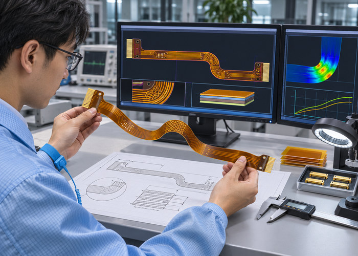
What Long Flexible PCB Manufacturing Capabilities Does BestFPC Offer?
BestFPC provides custom single-layer, double-layer, and other flexible PCB manufacturing services, with fabrication feasibility evaluated according to circuit dimensions, materials, and routing requirements.
| Manufacturing Parameter | BestFPC Capability |
|---|---|
| Maximum single-layer dimensions | 500 × 2000 mm |
| Maximum double-layer dimensions | 250 × 1380 mm |
| Base materials | PI, PET |
| Base-material thickness (excluding copper) | 12, 18, 25, 50, 75, 100, 125, 150 μm |
| Copper thickness range | 12–140 μm |
| Minimum trace width / spacing | 0.05 / 0.05 mm |
| Minimum hole diameter | 0.10 mm |
| Surface finish options | ENIG, Flash Gold, Hard Gold, ENEPIG |
| Stiffener materials | PI, FR4 |
Manufacturing feasibility depends on the combination of finished dimensions, layer count, copper thickness, and circuit features. Maximum board dimensions and minimum feature sizes require confirmation for each proposed construction.
Why Choose BestFPC as Your Long Flexible PCB Manufacturer?
BestFPC offers custom-length fabrication, free DFM support, precision connector-tail manufacturing, and prototype-to-production services. We help customers address nonstandard board dimensions, connector fit, manufacturing defects, and production consistency.
Our manufacturing advantages include:
-
Custom Lengths and Special Outlines: Manufacture extended, narrow, irregular, and customized flexible circuits according to approved drawings. This helps accommodate equipment structures that conventional-size flexible boards cannot fit.
-
Free DFM Check Before Fabrication: Review circuit dimensions, stackups, trace spacing, bending areas, coverlay openings, and stiffener construction. Identify potential manufacturing conflicts early to reduce avoidable design revisions, rework, and repeated prototyping.
-
Precision Connector-Tail Manufacturing: Fabricate ZIF contact tails, contact fingers, solder pads, and local reinforcement according to specified connector requirements. Controlled contact dimensions help reduce insertion problems and unreliable connections.
-
Material and Copper-Thickness Support: Evaluate manufacturable material constructions against current, circuit length, and mechanical requirements, helping avoid unsuitable combinations that could complicate fabrication.
-
Circuit and Dimensional Quality Control: Use incoming inspection, process checks, optical inspection, critical dimensional measurements, and electrical testing to help reduce open circuits, shorts, contact defects, and dimensional nonconformities.
-
Prototype and Volume Production: Support initial samples, small batches, and subsequent production using approved design revisions and specifications, allowing customers to verify the product before placing larger orders.
-
Quality Documentation Support: Provide applicable quality-management documentation and manufacturing inspection records according to project requirements, helping customers evaluate supplier qualifications and acceptance conditions.
Whether your project involves unusual dimensions, complex connector geometry, or tight installation tolerances, BestFPC can evaluate the manufacturing requirements and provide custom fabrication based on your confirmed specifications.

What Information Is Needed for a Long Flexible PCB Quotation?
For an accurate long flexible PCB quotation, provide Gerber files, finished dimensions, stackup specifications, connector requirements, and order quantity. Special bending or reliability requirements should also be included where applicable.
Please prepare the following information:
-
Gerber Files: Copper layers, drilling data, coverlay openings, circuit outline, and other required manufacturing files.
-
Finished Dimensions: Overall length, width, thickness, and critical dimensional tolerances.
-
Material Specifications: Layer count, PI thickness, copper thickness, and any special laminate requirements.
-
Mechanical Requirements: Bend locations, bending radius, installation conditions, and expected movement cycles.
-
Connector Specifications: Contact pitch, tail dimensions, surface finish, and stiffener requirements.
-
Order Information: Prototype or production quantity, required delivery date, and delivery destination.
-
Special Acceptance Requirements: Controlled impedance, bending-cycle qualification, dimensional tolerances, or specific inspection reports.
If your Gerber files are not yet complete, you can submit preliminary outlines, stackup information, and connector requirements for an initial manufacturing feasibility review.
FAQs About Long Flexible PCBs
Q1. Can long flexible PCBs be rolled for transportation?
A1. Some long flexible PCBs can be packaged in controlled coils, provided the bending radius meets the circuit's mechanical requirements. Packaging must prevent excessive compression, sharp folds, and localized damage.
Q2. Can electronic components be soldered directly onto a long flexible PCB?
A2. Yes. Components should generally be placed outside repeated-bend regions. Local stiffeners may be required to support solder joints and withstand assembly stresses.
Q3. What is the difference between a long flexible PCB and a flat flexible cable (FFC)?
A3. An FFC typically uses parallel conductors, while a long flexible PCB supports customized routing, branches, solder pads, and multiple contact configurations for more complex interconnection requirements.
Q4. Can pressure-sensitive adhesive be added to a long flexible PCB?
A4. Yes. Pressure-sensitive adhesive can be applied to specified mounting areas. Adhesive thickness, bonding surface, operating temperature, and bending conditions must be considered to avoid interfering with circuit flexibility.
Q5. Can EMI shielding be added to a long flexible PCB?
A5. Yes. Shielding films or suitable copper constructions can be evaluated according to electromagnetic compatibility requirements. Shielding coverage, grounding arrangements, and additional thickness must be compatible with the electrical and mechanical design.
Q6. Can long flexible PCBs use different connector types?
A6. Yes. Different connection points can accommodate ZIF tails, solder contacts, or other suitable interfaces, provided each connection meets its specified mechanical and electrical requirements.
Q7. Which surface finish is suitable for frequently mated connectors?
A7. Wear-resistant contact finishes, such as hard electroplated gold, are commonly considered for repeated mating. The required plating specification should follow the connector type, expected mating cycles, and contact-performance requirements.
Q8. How should long flexible PCBs be stored?
A8. Keep circuits in clean, dry protective packaging and avoid heavy compression, folding, or unnecessary bending. Products requiring subsequent soldering should also follow the storage requirements associated with their surface finish.
Get Your Custom Long Flexible PCB Manufactured by BestFPC
Are board-length limitations, excessive voltage drop, connector mismatches, or bending failures delaying your long flexible PCB project? BestFPC provides custom-length fabrication, precision connector-tail manufacturing, material and stackup support, and a free DFM check before production. We help identify manufacturing issues that could affect dimensional accuracy and connection reliability, reducing avoidable design changes, rework, and repeated prototyping.
Don't redesign your entire electrical interconnection system simply because conventional flexible PCB dimensions cannot meet your requirements. Send your Gerber files, circuit dimensions, connector specifications, order quantity, and delivery requirements to sales@bestfpc.com. Contact BestFPC for a custom manufacturing quotation and move your long flexible PCB project from drawings to prototypes and repeat production.


.png)
.png)
.png)
.png)

.png)