


 2026-10-15
 BEST
BESTAn ultrasound PCB must fit inside the probe while carrying transmit pulses, weak echo signals, or connections between electronic boards. Choosing the construction means balancing three needs: space for the assembled circuit, signal quality, and reliable interconnections.
For compact ultrasound probe projects, BestFPC offers DFM pre-review by engineers with 20 years of PCB/PCBA experience, plus prototype and small-batch support. Our integrated PCB fabrication, component sourcing, assembly, and testing services help you move from an approved design to a build for evaluation. Email your board outline and proposed stackup to sales@bestfpc.com to discuss construction options before prototyping.
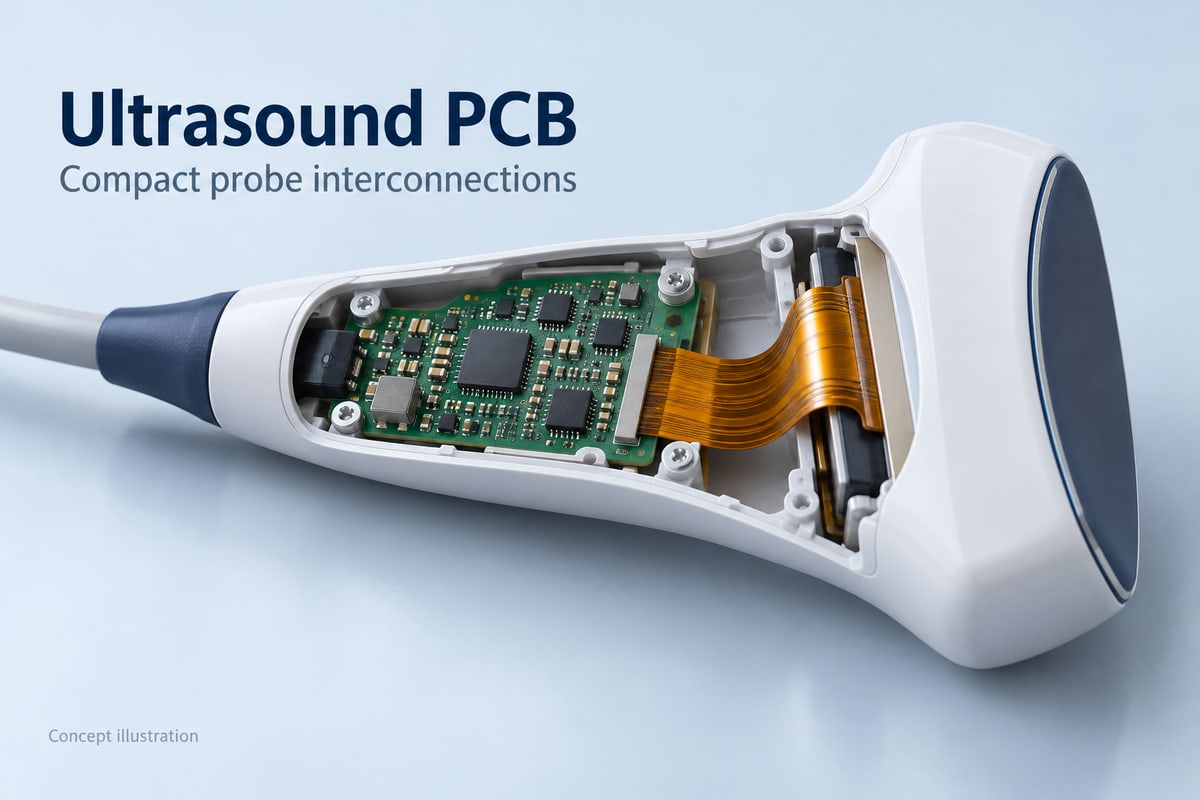
What Does an Ultrasound PCB Do Inside a Probe?
An ultrasound PCB connects the transducer to the electronics that drive it or process returning echoes. Its specific role depends on which functions are located inside the probe.
The main roles are:
- Transducer interconnection: Carry connections between the transducer array and the electronic assembly. A flex circuit can follow the available space around the probe structure.
- Transmit and receive electronics: Support the circuits that generate excitation pulses and handle returning electrical signals, where these functions are integrated into the probe.
- Power and board connections: Connect or support the power and processing sections used by the chosen architecture.
TI's smart-probe reference design uses separate signal-processing and power boards, with flex PCB connections for the transducer. It illustrates why the term ultrasound equipment PCB can cover several different board functions.
For a flex PCB for ultrasound probes, first identify the signals crossing the flex section. This helps avoid specifying a simple interconnect as though it were a fully populated processing board.
When Should Ultrasound PCBs Use Flex or Rigid-Flex?
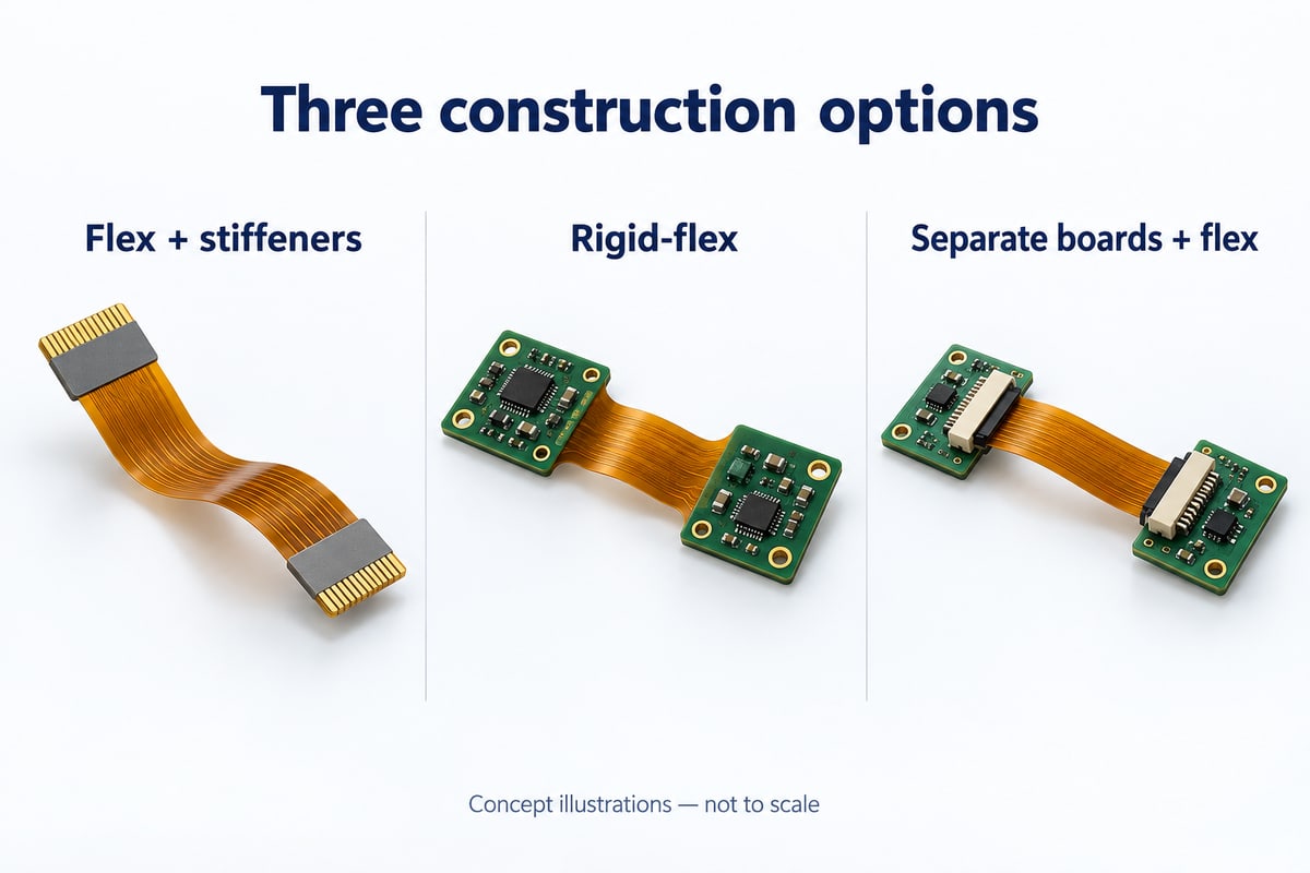
Choose flex for a shaped interconnect; consider rigid-flex when populated rigid sections need an integrated flexible connection. Separate boards remain useful when detachable interfaces or assembly access matter.
| Construction | Main benefit | Main constraint |
|---|---|---|
| Flex + stiffeners | Shaped routing | Supported ends |
| Rigid-flex | Integrated connections | Assembly geometry |
| Separate boards + flex | Detachable interfaces | Connector space |
The choice becomes clearer when tied to the probe layout:
- A narrow path around the transducer: A flex interconnect can follow the route, with local stiffeners supporting its terminations.
- Several populated sections in a confined housing: A rigid-flex PCB can join those sections without a separate connector at each integrated transition.
- Boards that must be fitted or disconnected separately: Separate boards and flex connections may suit the assembly sequence better, provided the connectors fit.
A stiffener supports a flex circuit mechanically; it does not turn it into an electrically interconnected rigid-flex construction. Compare the complete assembled shape, including connectors and reinforcement, rather than bare-board thickness alone.
How Can Ultrasound PCB Layout Reduce Receive-Channel Noise?
Keep interference from transmit, power, and digital circuits out of the receive path. A low-noise analog front end cannot compensate for every disturbance introduced around it.
Focus ultrasound PCB design on three connected issues:
- Signal return paths: Route signals with appropriate reference planes. TI's layout example uses adjacent ground references and ground vias where signals change reference planes.
- Channel coupling: Give neighboring channels sufficient routing separation for the design. Do not copy one reference board's spacing or layer count as a universal rule.
- Switching power placement: Evaluate supply switching loops near sensitive traces. Shielding alone cannot substitute for a suitable power and signal layout.
TI documents the reference-plane and routing approach, while Analog Devices explains how switching supply noise couples into ultrasound signal paths.
Follow the signal across the rigid board, connector, and flex section. A clean route on one board does not resolve a poor transition elsewhere in the assembly.
How Do Channel Count and Probe Size Affect the Stackup?
More channels increase routing demand, while a smaller probe limits the space available to carry those connections. Layer count must satisfy both the electrical layout and the mechanical envelope.
Three trade-offs drive the stackup:
- Routing density versus board area: More connections need routing space. The transmitter and multiplexer architecture affects how those connections are arranged.
- Reference planes versus total thickness: Signal layers and their reference planes must fit within the thickness available to the board assembly.
- Routing capacity versus bend space: Adding layers to the flexible section changes the construction that must pass through the bend. Keep that region as simple as the electrical requirements allow.
Two probes with similar transducer counts can therefore need different stackups. The useful target is a construction that carries the required channels and still fits the installation path—not a predetermined number of layers.
Where Should Flex Circuits Bend Inside an Ultrasound Probe?
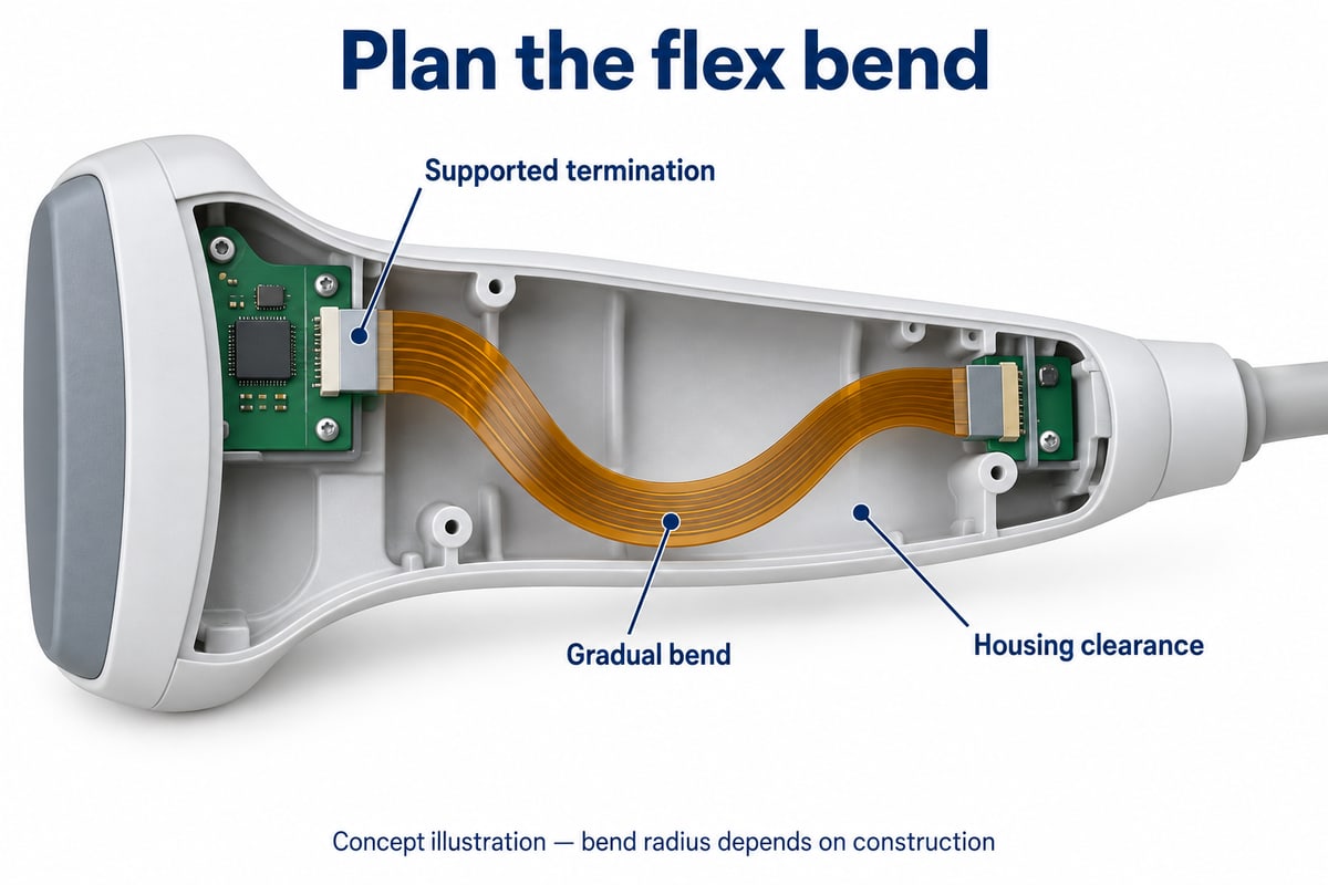
Place bends in dedicated flexible sections, away from supported component and connector areas. Decide whether the circuit bends only during installation or moves repeatedly in use before choosing its construction.
- Allow a gradual bend: Reserve enough housing space for the intended radius instead of forcing the circuit into a sharp crease.
- Keep plated through-holes out of the bend: Locate them in suitable areas outside the intended bending region.
- Plan the stiffener edge: Reinforcement supports terminations, but its edge also marks a change in flexibility. Position that transition deliberately. Poor bend placement can also contribute to flex PCB delamination, particularly near stiffener boundaries.
- Check the installation movement: During portable ultrasound PCB assembly, the flex must reach its final position without being sharply folded while adjacent boards are fitted.
The final shape is only part of the problem. A circuit that sits comfortably inside the closed housing can still be damaged by the route it takes during assembly.
How Does Heat Build Up in a Compact Ultrasound Probe?
Heat accumulates when losses in the transducer and electronics exceed the rate at which the assembly releases heat. PCB material selection alone does not establish an effective cooling path.
Separate the thermal problem into three parts:
- Heat sources: Transducer losses, electronic processing, and power conversion contribute to the load inside the probe.
- Heat paths: Determine how heat travels from those sources through the completed assembly. Do not assume a thin flex connection provides the main heat-removal path.
- Operating conditions: Assess the assembled probe under its intended use. Board temperature and probe surface temperature describe different parts of the thermal behavior.
A higher temperature-rated material may tolerate a different operating environment, but that rating does not show how efficiently heat escapes the enclosure. Thermal assessment must address the assembled device.
How Can BestFPC Support Your Ultrasound PCB Project?
BestFPC can support the flexible and rigid-flex manufacturing portion of your ultrasound PCB project, with assembly services agreed around the approved design.
For a compact probe, the manufacturing discussion can focus on:
- Stackup and routing requirements: Review the proposed construction alongside specified impedance or shielding needs.
- Bends and terminations: Discuss the flex outline, bend regions, and connector reinforcement in relation to the assembled probe.
- Assembly and inspection: Define the required component assembly, inspection, and testing against the project specification.
This connects the manufacturing review to how the circuit will fit within the probe. Board acceptance and system-level imaging validation remain separate tasks.
FAQs about ultrasound PCB
Is every ultrasound PCB flexible?
No. Ultrasound systems can use rigid boards, flexible interconnects, and rigid-flex assemblies. The construction depends on the board's function and location.
Does an ultrasound PCB always need a high-frequency laminate?
No single laminate follows from the application name. Select materials against the board's electrical, mechanical, thermal, and manufacturing requirements.
Is rigid-flex always better than a separate flex interconnect?
No. Rigid-flex can reduce separate interconnections. Separate boards may be preferable when detachable interfaces or assembly access are priorities.
Can a continuity test verify ultrasound image quality?
No. Continuity testing checks connections. Image quality depends on the transducer, signal chain, power, processing, and completed assembly, and needs system-level evaluation.
Planning a compact ultrasound probe? Send your Gerber files, proposed stackup, and assembly outline to sales@bestfpc.com for a manufacturing review and quotation. Include the BOM if component assembly is required, so BestFPC can assess the board construction and assembly scope together.


.png)
.png)
.png)
.png)

.png)