


 2026-10-14
 BEST
BESTFor engineers preparing a new build, reviewing these risks before fabrication helps connect material choices with assembly conditions. BestFPC provides FPC manufacturing and assembly support for prototypes and production. Send your proposed stackup and project requirements to sales@bestfpc.com to discuss manufacturing feasibility.
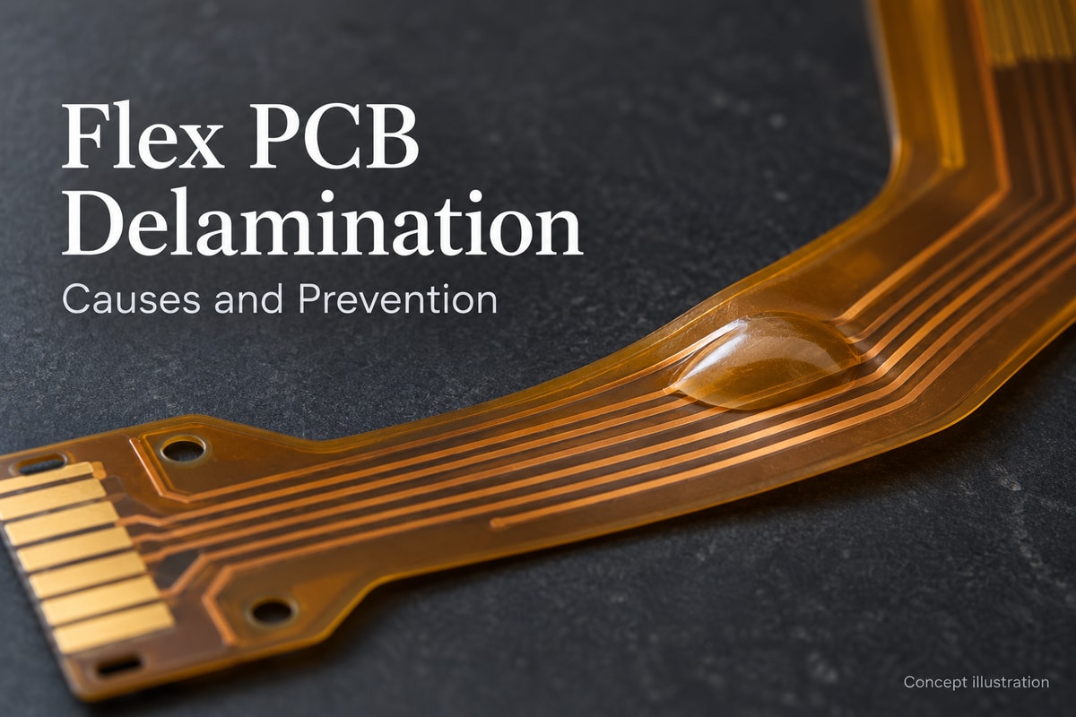
What Does Flex PCB Delamination Look Like?
Flexible circuit board delamination may appear as a raised bubble, a lifted film, or an opening between layers that should remain bonded. Some separation is internal and cannot be confirmed from a surface photograph.
The location helps narrow the investigation:
- Across the circuit surface: A blister or raised patch may indicate separation beneath the coverlay or at another interface. Its appearance alone does not identify the failed layer.
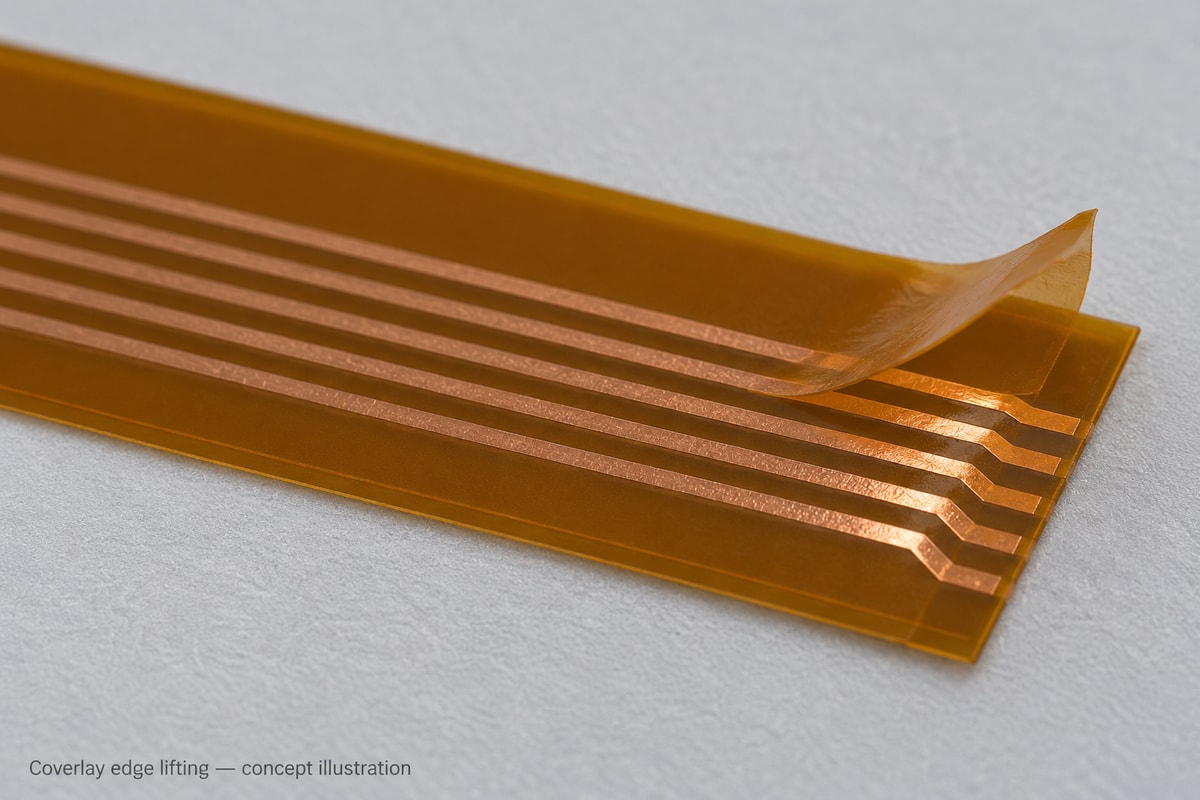
- Along a coverlay edge: Lifting can expose a previously covered area. Look for its relationship to openings, handling points, and bends.
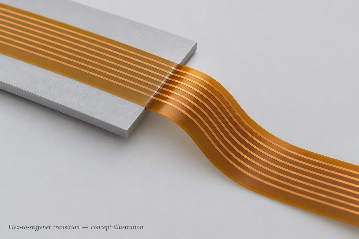
- Beneath a stiffener: An edge gap may involve the stiffener attachment rather than the copper-to-polyimide bond.
- Inside the construction: A section through the affected area may reveal separation that is difficult to see externally.
Record the defect before peeling, heating, or bending the sample further. Those actions can change the evidence. A surface wrinkle or color difference should prompt inspection, but neither automatically proves flex circuit delamination.
What Causes Flex PCB Delamination During Reflow?
Reflow can expose a weakness that was not visible on the incoming bare board. Moisture is a major concern for polyimide constructions, but weak bonding and unsuitable thermal exposure also deserve attention.
Three mechanisms should be investigated separately:
- Absorbed moisture: Polyimide moisture absorption can occur during storage and handling. Heating during soldering can turn retained water into vapor, creating pressure at bonded interfaces.
- Insufficient bonding: Poor surface preparation, contamination, voids, or an unsuitable lamination process can leave weak regions that separate under heat.
- Thermal exposure beyond the construction’s capability: The complete material system must tolerate the actual assembly process, including subsequent soldering and rework operations.
Delamination of PCB layers after reflow does not, by itself, prove that the oven temperature was too high. Compare material and lamination records, moisture exposure, and the measured product temperature profile before selecting a corrective action.
For rigid-flex designs, the rigid flex PCB manufacturing process also involves bonding materials and rigid-to-flex transitions that deserve attention when investigating delamination. For example, separation limited to a stiffener attachment deserves a different investigation from widespread blistering beneath the coverlay. Simply increasing the bake time may leave the underlying bonding problem unresolved.
Why Does Coverlay Delamination Occur Near Bend Areas?
Bending loads the bonded structure. If movement concentrates near a weak bond or an abrupt stiffness change, the coverlay interface can become a vulnerable point.
Pay particular attention to these features:
- Stiffener boundaries: The circuit changes from a supported section to a flexible section. Positioning the bend at that boundary can concentrate deformation.
- Tight or forced bends: A small bend radius or a fold imposed during installation can create more strain than the construction was intended to accommodate.
- Coverlay bonding around conductors: The adhesive must flow and fill the spaces around copper features appropriately during lamination.
- Repeated movement: A circuit that bends once during installation has different demands from one that moves throughout service.
Review the assembled motion path, including twisting and handling, rather than relying only on the flat drawing. Also distinguish coverlay delamination from a cracked copper trace: an intermittent open circuit does not establish which failure mechanism occurred.
Do Adhesiveless Flex PCBs Eliminate Delamination Risk?
No. An adhesiveless base laminate removes the separate adhesive layer between copper and the base film, but other bonded interfaces may remain in the finished circuit.
Review the complete construction:
- Base laminate: Confirm how the copper and dielectric are combined.
- Coverlay: A film coverlay may still use adhesive to encapsulate the conductors.
- Stiffeners and additional layers: Their attachment methods introduce separate material and process requirements.
Adhesiveless construction can be useful when thickness, flexibility, or thermal requirements justify it. It does not replace moisture control, sound coverlay bonding, or appropriate mechanical design. Select it for the project’s requirements rather than treating it as a universal cure for delamination.
How Can You Prevent Flex PCB Delamination Before Assembly?
Prevention combines a suitable manufactured construction with controlled handling before soldering. The fabrication team and assembler need compatible requirements.
Build prevention into these stages:
- Review the stackup before fabrication: Match the laminate, coverlay, bonding materials, and stiffener attachment to the intended soldering and bending conditions.
- Control the bonding process: Use material-specific lamination and curing conditions, with suitable surface preparation and adhesive coverage.
- Protect boards during storage: Follow the agreed packaging and environmental controls. Track opening and exposure where the handling procedure requires it.
- Define flex PCB pre-baking: Establish the drying process with the fabricator and assembler for the actual construction and surface finish.
- Control handling after drying: Avoid unmanaged delays that allow moisture to return before soldering. Keep drying and assembly timing coordinated.
A single bake temperature and duration should not be applied to every FPC. Thickness, copper coverage, stiffeners, oven loading, and finish sensitivity can affect the process. Excessive or repeated baking can also affect solderability.
Confirm the drying method and assembly profile on representative builds before relying on them for production.
How Is Flex PCB Delamination Confirmed and Evaluated?
Confirmation requires evidence of separation at an interface. Evaluation then asks how far it extends, what caused it, and whether the affected construction still meets its requirements.
Use each inspection or test to answer a specific question:
| Method | Practical question |
|---|---|
| Magnified visual inspection | Where does the visible defect begin, and how extensive is it? |
| Cross-section analysis | Which interface has separated at the sampled location? |
| Appropriate peel testing | How does the tested bond perform under a defined method and condition? |
| Electrical testing | Have continuity or insulation requirements been affected? |
| Representative thermal or bend testing | Does the proposed corrective action hold up under the intended conditions? |
A cross-section examines the selected location and consumes that sample. Peel results depend on the interface and test method. Neither should be interpreted without those limits.
Electrical acceptance alone does not demonstrate sound bonding. For a recurring issue, compare affected and unaffected samples, then evaluate the revised process against agreed acceptance criteria.
Can a Delaminated Flex PCB Be Repaired Reliably?
A visibly flattened blister or a restored electrical connection is not enough to demonstrate a reliable repair. The affected interface and the board’s service conditions determine whether a controlled repair is feasible.
Keep these limits clear:
- Drying removes moisture: It does not restore a separated bond.
- Local adhesive application changes the construction: Added material may alter thickness, stiffness, insulation, or movement.
- A static attachment and a dynamic bend region have different demands: A repair near repeated motion requires particular scrutiny.
- Internal separation can extend beyond the visible area: Surface appearance may underestimate the affected region.
Segregate suspect boards and obtain an engineering disposition before further assembly. Where bond integrity cannot be restored and verified under an approved procedure, replacement provides a clearer route to meeting the original requirements.
Why Choose BestFPC for Your Flex PCB Project?
BestFPC combines FPC manufacturing with assembly support, helping engineers review how material, construction, and processing choices fit together. For projects concerned about delamination, this coordination is useful from the first prototype through production.
- DFM review before fabrication: Experienced FPC engineers review the proposed construction and provide process compatibility advice, helping identify manufacturing concerns before samples are built.
- Integrated FPC and PCBA services: FPC fabrication, component sourcing, assembly, and agreed testing can be coordinated through one supplier, making fabrication and assembly requirements easier to align.
- Prototype and small-batch support: Engineering teams can obtain samples for assembly trials, mechanical evaluation, and application-specific validation before committing to a larger build.
- Engineering support through production: Keeping approved material and process requirements consistent helps teams assess the implications of later changes.
This approach supports a manufacturable design and a more informed transition from prototype evaluation to production. Inspection methods and acceptance requirements should be agreed for the particular project.
FAQs About Flex PCB Delamination
Can a flex PCB pass electrical testing and still have delamination?
Yes. Layer separation can exist while conductors remain continuous. Electrical testing and assessment of the bonded structure answer different questions; both may be needed.
Can delamination appear only after the second soldering operation?
Yes. Review the complete thermal history and the handling interval between operations. Additional heat exposure and renewed moisture absorption are relevant possibilities, but the failure interface still needs to be examined.
Does vacuum packaging mean pre-baking is unnecessary?
No. Packaging does not prove that the board is sufficiently dry for assembly. Follow the approved handling and drying procedure for the actual construction and exposure history.
Is every bubble caused by moisture?
No. Similar surface symptoms can result from trapped material, voiding, weak bonding, or other process problems. Establish the affected interface and supporting evidence before assigning the cause.
Does changing RA copper to ED copper, or vice versa, solve delamination?
The foil label alone does not resolve a bonding failure. Review the specific foil treatment, laminate system, interface preparation, and process conditions. A material substitution also needs evaluation against the circuit’s electrical and mechanical requirements.
Planning a new flex PCB build or reviewing a delamination concern? Contact sales@bestfpc.com with your Gerber files, stackup, quantity, and assembly requirements. For an existing defect, include clear photographs, its location, and the stage when it first appeared. BestFPC can review the manufacturing requirements and discuss suitable prototype or production support.


.png)
.png)
.png)
.png)

.png)