


 2026-10-22

 BEST
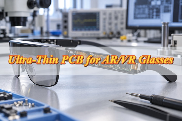
An ultra thin PCB allows AR/VR glasses to accommodate cameras, displays, sensors, and processing electronics within compact, lightweight frames. Thin rigid, flexible, and rigid-flex constructions serve different purposes depending on component placement, available space, and bending requirements.
Reducing PCB thickness also introduces challenges in mechanical strength, signal integrity, heat dissipation, and manufacturing reliability. Choosing suitable materials, stackups, and manufacturing processes helps prevent deformation, electrical failures, and unnecessary production costs.
Where Are Ultra-Thin PCBs Used in AR/VR Glasses?
Ultra thin PCBs are commonly used in temple arms, display modules, camera assemblies, sensor connections, and internal interconnections. Each location has different thickness, flexibility, and electrical requirements.
-
Temple Arms: House processing, power management, wireless communication, and control electronics inside narrow enclosures.
-
Display Modules: Connect microdisplays and driver circuits through compact, high-speed interconnections.
-
Camera Assemblies: Provide electrical connections for image sensors within restricted mounting spaces.
-
Sensor Modules: Support inertial, proximity, and other sensors where mounting stability and accurate positioning matter.
-
Hinges and Interconnections: Use flexible sections to connect electronic modules across curved or movable areas.
Rigid-flex construction is particularly useful when components require stable mounting areas while connections must pass through narrow or curved sections. It can also reduce the number of separate connectors and cables.
Which PCB Structure Is Best for AR/VR Glasses?
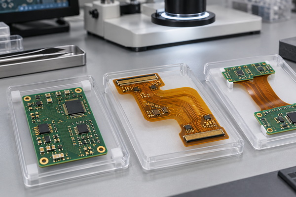
Ultra-thin rigid PCBs are suitable for fixed electronic modules, flexible PCBs accommodate curved interconnections, and rigid-flex PCBs combine both functions. The appropriate construction depends on mechanical movement, circuit density, and assembly requirements.
| PCB Structure | AR/VR Applications | Mechanical Properties | Main Advantages | Limitations |
|---|---|---|---|---|
| Ultra-Thin Rigid PCB | Display drivers, control boards, sensor modules | Thin, fixed structure requiring adequate support | Stable component mounting, multilayer routing, fine-pitch assembly | Limited bending tolerance; warpage risk when unsupported |
| Flexible PCB | Camera connections, frame interconnects, hinge wiring | Supports static bends or qualified repeated flexing | Lightweight, fits curved spaces, reduces separate wiring | Component areas may require stiffeners; bend life depends on construction |
| Rigid-Flex PCB | Temple assemblies, integrated sensor and processing modules | Rigid component areas connected by flexible sections | Reduces connectors and supports compact assemblies | Complex lamination, transition zones, higher fabrication cost |
HDI is an interconnection technology rather than a separate mechanical PCB category. Microvias and fine-line routing can be incorporated into rigid, flexible, or rigid-flex constructions when additional routing density is required.
How Thin Can an AR/VR Glasses PCB Be?
An ultra thin PCB for AR/VR glasses can be approximately 0.05 mm thick in selected flexible constructions, while thin rigid PCBs may be around 0.20–0.40 mm. Achievable thickness depends on PCB structure, layer count, copper thickness, and mechanical requirements.
-
Ultra-Thin Rigid PCB: Approximately 0.20–0.40 mm for selected thin constructions used in fixed electronic modules.
-
Single-Layer Flexible PCB: Approximately 0.05–0.20 mm, suitable for compact sensor circuits and interconnections.
-
Double-Layer Flexible PCB: Approximately 0.12–0.30 mm, providing additional routing capacity while maintaining flexibility.
-
Rigid-Flex PCB: Flexible and rigid sections have different thicknesses. Flexible regions may be around 0.10 mm, while rigid component areas require additional structural thickness.
BestFPC lists a minimum flexible PCB thickness of 0.05 mm for selected constructions. This provides an option for space-constrained electronics, although the achievable finished thickness depends on the approved materials, layer count, and manufacturing specifications.
For AR/VR glasses, thickness should be selected according to available installation space, required layer count, component support, and bending conditions. The completed stackup determines whether the target thickness can be manufactured consistently.
Which Materials and Stackups Work Best for Ultra-Thin PCBs?
Thin FR-4 laminates are suitable for rigid component areas, while polyimide-based materials are commonly selected for flexible and rigid-flex sections. Copper thickness, dielectric construction, and protective layers determine the finished thickness and mechanical performance.
| Material or Layer | Typical Options | Main Function | Selection Considerations |
|---|---|---|---|
| Thin FR-4 Core | Selected 0.10–0.20 mm cores | Supports rigid component areas | Thickness tolerance, thermal stability, copper balance |
| Polyimide Dielectric | 12.5–50 µm | Insulates flexible conductors | Flexibility, dimensional stability, thermal resistance |
| Copper Foil | 12–35 µm common options | Signal and power routing | Current capacity, fine-line capability, bend fatigue |
| Rolled-Annealed Copper | Multiple foil thicknesses | Conductors in demanding flex applications | Copper grade, fatigue performance, bending requirements |
| Adhesiveless Flex Laminate | Copper bonded without a separate copper-to-film adhesive layer | Enables thinner flexible cores | Laminate thickness, material compatibility, bonding quality |
| Coverlay | 12.5–25 µm polyimide film options, plus adhesive | Protects flexible conductors | Opening accuracy, adhesive thickness, bending performance |
| Stiffener | FR-4, polyimide, or metal | Supports connectors and components | Local rigidity, connector thickness, attachment method |
For example, a double-sided adhesiveless laminate with 18 µm copper / 25 µm polyimide / 18 µm copper has a nominal base thickness of 61 µm before additional processing and protective layers.
An ultra thin PCB carrying high-speed signals also requires suitable dielectric spacing and reference planes. The selected stackup must satisfy both mechanical constraints and the specified electrical performance.
How Can Bend Zones and Component Areas Be Made More Reliable?
Reliable bend zones require controlled bend radius, suitable copper routing, and mechanical separation between flexible sections and mounted components. A circuit bent once during installation has different fatigue requirements from one repeatedly moving inside a hinge.
-
Define Bending Conditions: Distinguish installation bending from repeated movement during operation.
-
Keep Components Outside Active Bend Zones: Avoid placing solder joints, rigid packages, and plated holes in areas exposed to repeated strain.
-
Control Conductor Geometry: Minimize sharp corners, abrupt trace-width changes, and copper discontinuities in bending regions.
-
Support Connector Areas: Use suitable stiffeners to prevent excessive deformation during insertion and removal.
-
Protect Rigid-to-Flex Transitions: Provide appropriate strain relief to reduce conductor cracking and delamination.
The rigid-to-flex transition is particularly vulnerable because mechanical stiffness changes abruptly. For moving hinges, bend-cycle testing should reproduce the expected radius, movement range, and operating life.
What Signal Integrity Challenges Affect Ultra-Thin AR/VR PCBs?
Ultra thin PCBs require accurate impedance control because reduced dielectric thickness changes the trace geometry needed for high-speed signal transmission. Camera and display interfaces are particularly sensitive to routing dimensions, reference planes, and signal transitions.
AR/VR glasses may use MIPI CSI-2 and DSI interfaces for image sensors and displays. Some MIPI D-PHY implementations specify approximately 100 Ω differential impedance, although the actual target and tolerance depend on the selected components and interface specifications.
In rigid-flex constructions, signals may cross sections with different dielectric materials or reference-plane arrangements. Poorly controlled transitions can create impedance discontinuities and unwanted reflections.
Power routing also requires attention. Thin copper traces have limited cross-sectional area, making voltage drop and conductor heating relevant in compact electronic modules.
Controlled trace geometry, dielectric thickness, and continuous return-current paths help maintain high-speed signal performance within the limited PCB area.
How Can Heat Be Managed in an Ultra-Thin AR/VR PCB?
Heat can be managed by spreading it through suitable copper areas and transferring it into designated mechanical cooling structures. Processors, power-management devices, and display drivers can generate concentrated heat inside narrow glasses frames.
Several approaches can improve thermal performance:
-
Copper Planes: Spread heat across supported PCB regions.
-
Thermal Vias: Transfer heat between layers where rigid construction permits.
-
Thermal Interface Materials: Connect heat-spreading areas to suitable mechanical structures.
-
Component Placement: Reduce thermal concentration where electrical and mechanical requirements allow.
Increasing copper thickness is not always beneficial. Thicker copper adds weight and can reduce flexibility, especially in bend regions.
Thermal simulation and assembled-product temperature measurements should confirm component temperatures and the effectiveness of the intended heat-transfer path.
What Are the Main Challenges in Ultra-Thin PCB Manufacturing?
Warpage, layer misalignment, microvia defects, and deformation during assembly are major challenges in ultra thin PCB manufacturing. Thin boards have limited stiffness, making fabrication and handling more demanding.
-
Thin-Panel Warpage: Unsupported panels may deform during drilling, imaging, and thermal processing. Copper balance and suitable panel support help maintain dimensional stability.
-
Layer Registration: Multilayer and rigid-flex boards require accurate alignment during lamination. Material movement or uncontrolled resin flow can affect critical dimensions.
-
Microvia Reliability: HDI fabrication requires controlled laser drilling, hole preparation, and copper metallization to prevent weak interconnections.
-
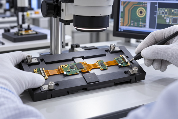
SMT Assembly Stability: Thin rigid and flexible boards may require carriers during solder paste printing, placement, and reflow to prevent movement and soldering defects.
Assembly support should be considered before fabrication is finalized. A thin PCB may meet bare-board specifications but still require additional fixtures or reinforcement for reliable fine-pitch assembly.
How Are Ultra-Thin AR/VR PCBs Tested for Quality and Reliability?
Ultra thin PCB quality is verified through electrical testing, dimensional inspection, structural examination, and mechanical qualification when bending is required. Testing must cover manufacturing quality and the intended operating conditions.
-
Electrical Testing: Detects open circuits and unintended shorts.
-
Dimensional Inspection: Verifies finished thickness, outlines, hole positions, and specified tolerances.
-
Automated Optical Inspection: Identifies conductor pattern defects within the inspection system's capabilities.
-
Microsection Analysis: Examines plated holes, microvias, copper thickness, and internal layer structures.
-
Impedance Testing: Verifies specified controlled-impedance structures.
-
Bend Testing: Evaluates flexible regions under defined bending conditions and cycle requirements.
After assembly, solder joint inspection, selected X-ray examination, and agreed functional testing can verify PCBA quality.
Applicable standards include IPC-6012 for rigid PCBs, IPC-6013F for flexible and rigid-flex PCBs, and IPC-A-610 for electronic assemblies. The acceptance class, standard revision, and additional testing requirements should be agreed upon before production.
What Affects the Manufacturing Cost of Ultra-Thin AR/VR PCBs?
Ultra thin PCB manufacturing cost depends mainly on material selection, layer count, HDI complexity, thickness tolerances, production yield, and assembly requirements.
-
Materials: Specialized thin laminates and adhesiveless polyimide can increase material costs.
-
Layer Count and HDI: Additional layers, microvias, and lamination cycles increase processing requirements.
-
Tolerances: Tight thickness and dimensional specifications can reduce manufacturing yield.
-
Panel Utilization: Irregular outlines and fragile flexible regions may increase material waste.
-
Assembly: Fine-pitch components, support fixtures, and specialized inspection can add production costs.
A rigid-flex PCB may cost more to fabricate than a thin rigid PCB but can eliminate separate connectors and assembly operations. Conversely, ultra-thin rigid construction may be more economical when components remain in fixed mounting areas.
Avoiding unnecessary HDI features, excessive layers, and overly restrictive tolerances can reduce manufacturing costs without compromising required performance.
How Should You Evaluate an Ultra-Thin PCB Manufacturer?
Choose an ultra thin PCB manufacturer that can demonstrate repeatable fabrication, controlled assembly, and reliable quality inspection for the required construction.
Before selecting a supplier, verify:
-
Manufacturing Capability: Supported board thickness, layer count, copper weight, line width, spacing, and drilling tolerances.
-
Rigid-Flex Experience: Ability to control flexible sections, rigid-to-flex transitions, and required HDI structures.
-
DFM Review: Evaluation of stackup, bending areas, panelization, and assembly feasibility.
-
Assembly Support: Suitable fixtures, fine-pitch placement, reflow control, and inspection methods.
-
Quality Documentation: Material records, test reports, applicable certifications, and production traceability.
Compare quotations using identical fabrication drawings, approved materials, acceptance standards, and testing requirements. Prototype inspection results and documented process capability provide stronger evidence of manufacturing reliability than minimum-thickness claims alone.
Why Choose BestFPC for AR/VR Glasses PCB Manufacturing and Assembly?
BestFPC specializes in flexible and rigid-flex PCB manufacturing, providing custom fabrication, DFM review, prototyping, and assembly services for compact electronic products. With over 20 years of industry experience, BestFPC supports projects requiring thin constructions, complex interconnections, and reliable component assembly.
For AR/VR glasses PCB projects, BestFPC offers:
-
Ultra-Thin Flexible PCB Manufacturing: Supports selected flexible PCB constructions down to 0.05 mm, subject to stackup and manufacturing feasibility.
-
Custom Rigid-Flex PCB Fabrication: Combines mechanically stable component areas with flexible interconnections for space-constrained assemblies.
-
Material and DFM Review: Evaluates polyimide materials, copper thickness, stackups, bend regions, stiffeners, and fabrication tolerances.
-
FPC Assembly Services: Provides component sourcing, SMT assembly, and inspection for flexible and rigid-flex PCB projects.
-
Prototype to Volume Production: Supports sample fabrication, manufacturing review, and repeat production requirements.
-
Quality Control: Uses incoming material checks, in-process inspection, electrical testing, and applicable assembly inspection methods.
BestFPC is a China-based flexible PCB manufacturer supplying international OEM and ODM customers. Its services help customers coordinate flexible PCB fabrication and component assembly through one manufacturing partner.
For your AR/VR glasses project, send Gerber files, PCB stackup, finished thickness, bend-radius requirements, BOM, assembly drawings, and estimated quantities to sales@bestfpc.com for DFM review and a custom quotation.
Common Questions About Ultra-Thin PCB Applications
Q1: Can an ultra thin PCB withstand lead-free reflow soldering?
A1: Yes. An ultra thin PCB can withstand lead-free reflow when its materials and construction support the required temperature profile. Thin boards may require SMT carriers to prevent deformation during soldering.
Q2: Is laser depaneling suitable for thin flexible circuits?
A2: Yes. Laser depaneling minimizes mechanical stress and supports precise cutting of flexible circuits. Laser settings must be controlled to prevent edge damage, excessive heating, and material discoloration.
Q3: How should ultra-thin PCBs be packaged for international shipping?
A3: Use rigid supports, protective separators, and suitable moisture protection to prevent bending, compression, and contamination. Flexible circuits should not be folded below their specified minimum bend radius.
Q4: What is the difference between coverlay and flexible solder mask?
A4: Coverlay is a bonded insulating film, while flexible solder mask is a protective coating. Coverlay is commonly preferred for demanding bending applications, although both materials require appropriate mechanical qualification.
Q5: Can V-scoring be used to separate ultra-thin PCBs?
A5: V-scoring may be suitable for certain thin rigid PCBs, but separation stress can cause cracking or deformation. Flexible circuits generally use methods such as laser cutting or die cutting.
Q6: Should flexible PCBs be baked before SMT assembly?
A6: Not always. Baking depends on moisture exposure, material construction, and storage conditions. Follow the material supplier's instructions because excessive heating may damage adhesives or affect dimensional stability.
Q7: How is ESD controlled during ultra-thin PCB assembly?
A7: Use grounded equipment, ESD-safe workstations, controlled handling, and protective packaging. These measures protect sensitive electronic components from electrostatic discharge during PCB assembly and inspection.
Q8: Does conformal coating affect flexible PCB bending performance?
A8: Yes. Coating thickness and stiffness can reduce flexibility or cause cracking during repeated bending. Select a coating qualified for the required bend radius and operating conditions.
Q9: Can ZIF connectors accept flexible PCBs with different thicknesses?
A9: Only within the connector's specified mating-thickness range. Stiffeners can adjust the finished insertion thickness to achieve reliable contact and prevent connector damage.
Q10: Can EMI shielding film be added to an ultra-thin flexible PCB?
A10: Yes. EMI shielding film can reduce electromagnetic interference, but it adds thickness and may increase bending stiffness. Grounding, adhesion, and flexibility must be verified for the intended application.
Conclusion
An ultra thin PCB for AR/VR glasses must balance finished thickness, electrical performance, mechanical durability, and manufacturing stability. Thin rigid boards are suitable for fixed electronics, while flexible and rigid-flex constructions accommodate compact interconnections and bending requirements. Material selection, stackup accuracy, mechanical support, and process control determine manufacturing reliability.
If you are looking for custom ultra thin PCB manufacturing, OEM/ODM production support, prototyping, or volume flexible PCB assembly, BestFPC offers manufacturing and technical support for your project. Send your Gerber files, BOM, technical drawings, and estimated quantities to sales@bestfpc.com for a manufacturing review and quotation.


.png)
.png)
.png)
.png)

.png)