


 2026-11-19

 BEST
A transceiver PCB carries the circuitry that transmits and receives signals. Depending on the application, it may support an optical module, an RF link, or an industrial interface such as CAN. Flexible and rigid-flex constructions help connect these circuits within compact assemblies, but the board structure must match the electrical interface and installation requirements.
At BestFPC, we manufacture flexible and rigid-flex circuits to customer-approved designs, with PCB assembly available for a coordinated build. Our engineers provide DFM review reports and BOM optimization recommendations, while sample and small-batch production supports development before volume release. Send your drawings to sales@bestfpc.com to discuss the stackup, interconnect structure, and assembly scope for your transceiver project.
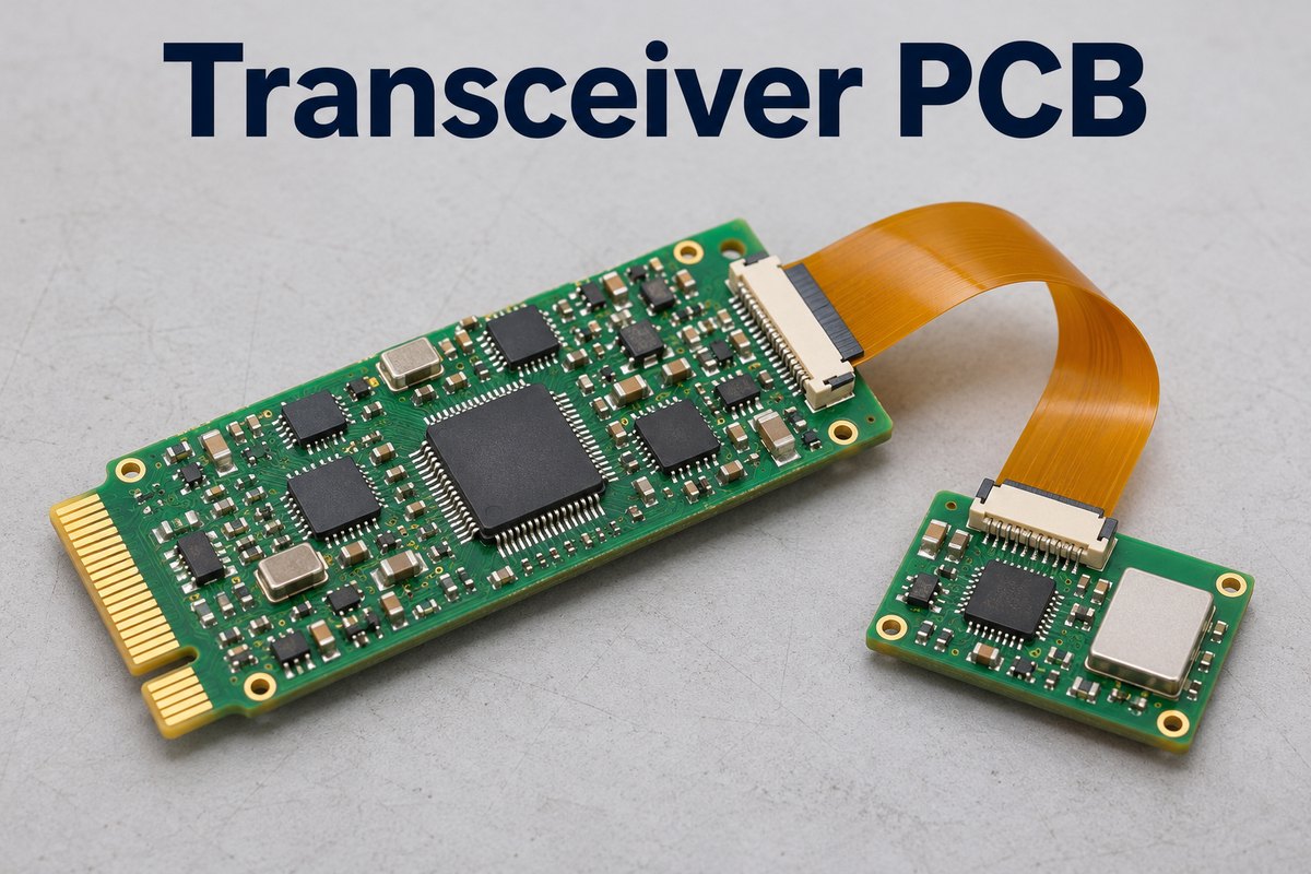
What Transceiver PCB Types Can BestFPC Manufacture?
We manufacture custom FPC and rigid-flex boards that can serve as transceiver interconnects or carry interface electronics. The choice depends on whether your assembly needs a separate flexible link, supported component areas, or an integrated rigid-flex structure.
| Board Structure | Suitable Project Need | Detail to Confirm |
|---|---|---|
| Single- or double-sided FPC | Short connections with limited routing complexity | Pin count, return path, installed bend |
| Multilayer FPC | Denser routing or additional reference layers | Approved stackup and electrical requirements |
| Rigid-flex PCB | Component-bearing rigid sections connected through flex | Rigid-to-flex transitions and housing fit |
| Locally reinforced FPC | Flexible routing with supported terminals or components | Finished thickness at each reinforced area |
An optical module may need a short flex connection between its electronic sections. A CAN bus transceiver PCB may instead use a rigid component area and a flexible connection to a remote connector. These applications require different routing and verification criteria; one stackup should not be assumed suitable for both.
The order can cover bare circuits or an assembled board. A populated circuit board and a complete qualified transceiver module are separate deliverables.
Transceiver PCB Manufacturing Capabilities
Our manufacturing options cover PI-based flexible circuits and multilayer rigid-flex structures. We review the requested materials, copper geometry, reinforcement, and impedance requirements together before approving a production stackup.
| Manufacturing Item | Available Option |
|---|---|
| FPC layer count | 1–4 layers |
| Rigid-flex layer count | 2–20 layers |
| Adhesive PI core | 0.5, 1, or 2 mil |
| Adhesiveless PI core | 0.5, 1, 2, or 3 mil |
| Rigid-flex impedance tolerance | ±10% |
| Surface finish | ENIG, gold plating, OSP, tin plating |
These options do not establish that every combination can be produced together. Finished board thickness includes the relevant copper, dielectric, adhesive, and coverlay layers; it should not be inferred from PI film thickness alone.
For a high-speed transceiver logic PCB, provide the interface specification, target impedance, material requirements, and any loss or skew limits. We use these requirements to review manufacturability. A controlled-impedance specification alone does not establish the supported data rate or qualify the complete signal channel.
Optical Transceiver PCB Interconnects for Compact Modules
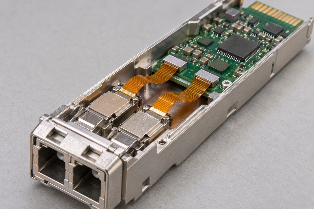
An optical transceiver PCB interconnect can accommodate offsets between electronic sections while preserving the required terminal locations. We manufacture the flexible connection to the approved electrical and mechanical definition, including its installed shape and locally supported areas.
Key manufacturing decisions include:
- Routing space: Define the available path, installed bend, and clearance from the housing. Keep solder joints and reinforced terminal regions outside the intended bending section.
- Electrical construction: Specify which connections carry high-speed signals, control signals, or power. Match the stackup and conductor geometry to each requirement rather than treating every connection as an identical flex tail.
- Terminal fit: Control the finished thickness, contact dimensions, and stiffener placement where the circuit meets its connector or mating board.
- Heat exposure: Identify nearby heat sources and assembly temperatures so that material and adhesive choices can be reviewed against the actual environment.
For a fiber optic transceiver PCB, the internal flexible connection and the module’s external electrical interface should be defined separately. The connection from an SFP transceiver PCB to its SFP electrical connector must follow the applicable mechanical and contact specification; a standard flexible tail is not automatically an SFP edge interface.
When reviewing an optical transceiver PCB design for manufacture, we focus on the supplied stackup, geometry, and production tolerances. Optical alignment and complete module qualification require their own processes and acceptance criteria.
DFM Review for CAN Transceiver PCB Layout
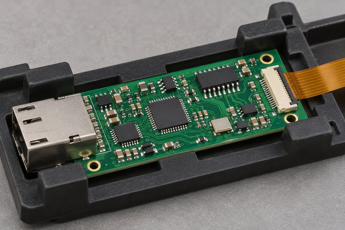
Our DFM review for CAN transceiver PCB layout checks whether the supplied board can be fabricated and assembled consistently. It addresses manufacturing constraints around the transceiver, connector, protection components, and any flexible transition.
- Footprint compatibility: Compare the selected component package with pad dimensions, solder-mask openings, and exposed-pad features where present.
- Connection geometry: Review trace widths, clearances, vias, and transitions against the approved stackup. Connector pin assignments must agree across the schematic, layout, and assembly documentation.
- Protection-component placement: Flag manufacturing or access conflicts around the protection and filtering components specified by the design engineer. Their electrical arrangement should follow the selected transceiver’s guidance.
- Mechanical separation: Keep the intended bend region distinct from solder joints, connector bodies, and local reinforcement boundaries.
- Assembly access: Check whether placement, soldering, inspection, and the planned test connections remain accessible inside the panel and final assembly.
The DFM report identifies drawing or process issues for your engineer to resolve. It does not replace CAN network design, termination selection, or EMC validation.
Transceiver PCB Assembly to Your Approved Design
We coordinate PCB manufacture, component sourcing, and assembly using your approved BOM and production files. This gives your team one manufacturing interface for the bare circuit and the populated board.
The assembly plan covers:
- BOM control: Check package variants, temperature grades, availability, and approved alternatives. Changes to transceivers, references, or other performance-critical components require customer approval.
- Board support: Plan carriers and local reinforcement to support flexible areas during placement and soldering.
- Process compatibility: Review component temperature limits, moisture handling, and cleaning restrictions before selecting the assembly process.
- Configuration: Define firmware loading, programming connections, and any configuration steps included in the order.
A PCB-mount fiber-optic transceiver listed in the BOM must be assessed using its exact part number and mounting instructions. Assembling a packaged optical component onto a board is different from constructing and aligning an optical engine.
How Is Transceiver PCBA Quality Verified?
Transceiver PCBA quality is verified against agreed fabrication, assembly, and functional acceptance criteria. Each inspection answers a different question, so the test plan should identify both the required checks and their limits.
| Check | What It Evaluates | Required Basis |
|---|---|---|
| Bare-board electrical test | Opens and shorts | Approved netlist |
| Dimensional inspection | Outline, holes, and terminal fit | Drawing and tolerances |
| Impedance verification, when specified | Selected controlled-impedance structures | Approved targets and test method |
| Assembly inspection | Placement and solder-joint workmanship | Assembly acceptance criteria |
| Functional testing, when agreed | Circuit response under defined conditions | Fixture, procedure, and limits |
Inspection methods should match the component packages and accessible features. Where a joint cannot be assessed directly, the inspection plan must specify an appropriate method rather than assume a visual check is sufficient.
High-speed link testing, optical power measurement, receiver sensitivity, and system-level EMC are separate verification tasks. Include them explicitly when required, together with equipment, responsibility, and acceptance limits. Passing a bare-board test does not demonstrate complete transceiver performance.
Prototype Transceiver Boards for Engineering Validation
We support prototype transceiver boards and small batches so your engineers can evaluate the manufactured structure before volume release. The prototype plan should identify which mechanical and electrical requirements each revision will assess.
- Confirm the production definition. Approve the stackup, outline, terminal thickness, reinforcement, and component revision before fabrication.
- Check installation fit. Evaluate flex routing, connector engagement, component clearance, and housing contact in the intended assembly.
- Validate the interface. Test the populated board with the selected components and representative operating conditions using your agreed validation plan.
- Release a controlled revision. Update fabrication files, BOM, assembly drawings, and acceptance criteria together before the next build.
Record mechanical and electrical changes separately. This helps the engineering team identify the cause of a changed result instead of comparing builds with several undocumented differences.
How Quickly Can Transceiver PCBA Be Delivered?
Our PCBA quick-delivery option can support eligible projects in approximately 1.5 weeks, subject to material readiness, approved files, and process requirements. We confirm the schedule against the specific transceiver build rather than applying one lead time to every configuration.
- Material readiness: Special laminates, selected transceiver ICs, or module connectors may determine the earliest production date.
- Engineering release: Stackup, component substitutions, and mechanical questions need resolution before the build can proceed as planned.
- Test preparation: Custom fixtures, firmware, or interface-testing arrangements may require work beyond standard board manufacture and assembly.
The quotation should distinguish production time from additional qualification work and shipping. This makes the expected delivery milestone clear for both the engineering and purchasing teams.
Case Study: Flexible Interconnect for an Optical Transceiver Module PCB
A two-layer FPC we have manufactured provides a useful structural basis for an optical transceiver module PCB interconnect. Its thin routing section, reinforced terminals, and specified impedance requirement illustrate how a flexible connection can be defined for a compact module.
Application
The application uses a short flexible connection between electronic sections within the module. The routing section accommodates their relative positions, while reinforced ends support termination. Electrical suitability depends on the approved channel design and the final installed geometry.
Manufacturing Challenges
- Thin construction: The flexible region needs a controlled thickness while accommodating the specified copper and coverlay.
- Terminal support: The termination areas need a different mechanical structure from the flexible span.
- Electrical consistency: The impedance requirement must be translated into an approved stackup and conductor geometry.
BestFPC Manufacturing Solutions
- Defined material construction: The selected board specification combines adhesiveless PI with ED copper and yellow coverlay.
- Local reinforcement: PI stiffening supports the terminal area without extending reinforcement across the complete flexible section.
- Preproduction review: Production data and the layer structure are submitted for approval, with impedance details checked against the corresponding drawing.
Customer Benefits
This construction gives the module engineer a thin interconnect with locally supported ends and a clear electrical requirement to validate. It allows the flexible span and termination areas to be reviewed separately instead of compromising both with one uniform thickness.
PCB Specifications
| Parameter | Selected Board Specification |
|---|---|
| Structure | Two-layer FPC |
| PI material | 20 µm, adhesiveless |
| Copper | 20 µm ED copper |
| Coverlay | 0.5 mil, yellow |
| Flexible-region thickness | 0.11 ± 0.03 mm |
| Specified top-side reinforced area | FPC plus PI stiffener: 0.30 mm |
| Surface finish | ENIG |
| Impedance requirement | 100 Ω; geometry per drawing |
Why Choose BestFPC as Your Transceiver PCB Supplier?
BestFPC combines engineering review, circuit manufacture, and assembly coordination to help OEM teams turn an approved design into a controlled build. For customers selecting an optical transceiver PCB manufacturer, our contribution centers on the specified board and interconnect rather than an assumed complete optical-module service.
- Certified Quality Systems: Our qualifications include ISO 9001, ISO 13485, IATF 16949, and AS9100D. We align the applicable manufacturing-site and certification scope with project requirements; management-system certification is distinct from finished-product qualification.
- Experienced Engineering Support: Our team includes R&D and PCB/PCBA engineers with 20 years of experience. DFM reports and process recommendations give your engineers specific manufacturing issues to resolve before release.
- Integrated Production Resources: Our own PCB and PCBA factories, supported by more than 1,000 supply-chain partners, coordinate board fabrication, sourcing, and assembly through one project team.
- Development Support: Samples and small batches help your team evaluate installation and integration before increasing order quantities.
- Digital Traceability: Our digital workshop supports retrieval of material and product-batch information, production-cycle details, and progress within five seconds, helping the team investigate batch questions and track production.
FAQs about Transceiver PCB
Is a PCB for a fiber-optic transceiver the same as a complete module?
No. The PCB provides electrical connections and mounting features. A complete module also includes its specified electronic and optical components, mechanical parts, and qualification requirements. Define bare-board, PCBA, and complete-module supply separately.
Can every flexible PCB carry high-speed transceiver signals?
No. Suitability depends on the complete channel, including materials, routing, reference structures, transitions, and connectors. Layer count or impedance tolerance alone cannot establish a supported data rate.
Does a LIN transceiver PCB layout always need an inductor?
No universal inductor requirement applies to every LIN implementation. Use the selected device’s application circuit and the project’s EMC requirements to determine filtering. LIN and CAN layouts should not be treated as interchangeable.
Does AS9100D certification qualify a satellite transceiver PCB for flight?
No. AS9100D concerns the quality management system. A satellite transceiver PCB project needs its own material, workmanship, traceability, environmental, and acceptance requirements. Flight qualification cannot be inferred from the supplier’s certificate alone.
Can copper geometry be changed during manufacturing to meet impedance?
Any proposed change affecting the approved electrical or mechanical design should be reviewed with the customer. Agree on the adjustment and update the production documentation before release rather than making an unrecorded substitution.
Can an RF transceiver board and an optical module use the same material?
Possibly, but shared terminology does not establish material suitability. The operating requirements, routing lengths, loss limits, assembly conditions, and mechanical constraints must be assessed for each design.
For your next transceiver PCB project, our engineers can provide a DFM review report, coordinate approved BOM sourcing with PCB assembly, and support sample builds before volume production. These services help your team resolve manufacturing details while retaining control of circuit design and system validation. Send your drawings and build requirements to sales@bestfpc.com to begin the review.


.png)
.png)
.png)
.png)

.png)