


 2026-10-22

 BEST
A telecom flexible PCB board provides compact electrical connections for 5G antennas, RF modules, optical communication modules, and network equipment. Its flexible construction fits circuits into tight spaces, but signal performance, material selection, and bending requirements determine whether it is suitable for a particular device. An RF antenna connection and a low-speed control circuit may require very different flexible PCB structures, even within the same communication system.

Where Are Telecom Flexible PCB Boards Used in Communication Equipment?
Telecom flexible PCB boards are used in antennas, RF modules, optical communication equipment, and wireless devices where space-saving electrical connections are required. Common applications include:
-
5G Base Stations and Small Cells: Selected antenna feed circuits and internal RF connections where installation space is limited.
-
RF Antenna Modules: Flexible antenna elements and transmission lines that fit compact or curved installation areas.
-
Optical Transceiver Modules: Short internal connections between optical and electronic components in densely packed modules.
-
Routers and Wireless Gateways: Antenna connections, displays, and internal module interconnections that reduce separate wiring.
-
IoT Communication Devices: Compact antenna connections and lightweight circuit interconnections in wireless terminals.
FPC antennas are especially useful in space-constrained wireless equipment, where antenna placement is restricted by the enclosure or nearby components. Multilayer flexible and rigid-flex PCBs can also connect electronic modules arranged at different positions inside the equipment. Each application places different demands on signal performance, grounding, and mechanical flexibility.
What Electrical and Mechanical Requirements Should You Specify?
A telecom flexible PCB board must meet the signal performance and mechanical requirements of the equipment. The main specifications include:
-
Operating Frequency: Define the frequency range and signal type. High-frequency RF connections require closer attention to dielectric properties and transmission-line performance than low-speed control circuits.
-
Characteristic Impedance: Specify the target impedance and tolerance. 50 Ω is common in RF systems, while high-speed differential interfaces may require 90 Ω, 100 Ω, or other values according to their specifications.
-
Signal Loss and Interference: Establish acceptable insertion loss, return loss, and signal isolation for critical RF or high-speed connections.
-
Bending Requirements: Define the minimum bend radius, bending direction, and whether the board will be bent once during installation or repeatedly during operation.
-
Installation Constraints: Confirm the available space, connector positions, board thickness, and areas requiring mechanical reinforcement.
-
Environmental Conditions: Specify operating temperature, humidity exposure, and vibration requirements, particularly for outdoor communication equipment.
Electrical requirements and mechanical constraints should be established before selecting the final flexible PCB stackup. A structure that meets the routing requirements may still be unsuitable if its thickness or bending characteristics conflict with the installation conditions.
How Do You Choose the Right Flexible PCB Structure for Telecom Equipment?
Choose the flexible PCB structure according to circuit density, grounding requirements, and installation space. Single-sided and double-sided boards handle many simple connections, while multilayer and rigid-flex constructions support more complex layouts.
| PCB Structure | Suitable Telecom Applications | When to Choose |
|---|---|---|
| Single-Sided Flexible PCB | Simple antenna patterns and low-density interconnections | One conductive layer provides sufficient routing |
| Double-Sided Flexible PCB | RF connections, antenna modules, and control circuits | Additional routing or a reference conductor is required |
| Multilayer Flexible PCB | High-density communication modules and complex interconnections | More signal, power, or reference layers are needed |
| Rigid-Flex PCB | Wireless equipment with fixed component areas and flexible connections | Rigid mounting sections and flexible interconnections must be integrated |
For compact RF modules, a double-sided flexible PCB may provide sufficient routing and a controlled reference conductor without the thickness of a multilayer construction. Additional layers become necessary when signal routing, grounding, or circuit density cannot be accommodated in a simpler stackup.
A rigid-flex PCB is worth considering when several circuit sections must fit into different orientations. However, if the only requirement is to reinforce a connector, a conventional flexible PCB with a local stiffener may be sufficient.
Which Flexible PCB Materials Are Suitable for Your Telecom Application?
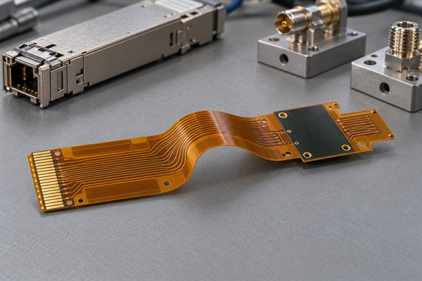
Polyimide (PI) is widely used in telecom flexible PCB boards, while low-loss PI and liquid crystal polymer (LCP) are options for applications with more demanding high-frequency requirements. The choice depends on operating frequency, acceptable signal loss, mechanical flexibility, and the overall circuit construction.
| Material | Main Characteristics | Suitable Telecom Applications |
|---|---|---|
| Standard Polyimide (PI) | Good flexibility, thermal stability, and broad availability | Control circuits, internal connections, and RF circuits that meet the required loss budget |
| Low-Loss Polyimide | Available in formulations with reduced dielectric loss | Selected high-frequency RF and high-speed interconnections |
| Liquid Crystal Polymer (LCP) | Low moisture absorption and low dielectric loss in suitable grades | High-frequency antennas and selected millimeter-wave modules |
Standard PI can be sufficient for control circuits and short internal connections, even when the equipment operates on a 5G network. More specialized materials become necessary when transmission loss or environmental requirements exceed the performance of a conventional construction.
For RF signal paths, the material's dielectric constant (Dk) and dissipation factor (Df) affect impedance and dielectric loss. Copper roughness, trace geometry, and dielectric thickness also influence performance. These properties should be assessed at the intended operating frequency, since choosing a low-loss material alone does not guarantee a low-loss circuit.
Why Choose BestFPC for Your Telecom Flexible PCB Project?
BestFPC brings over 20 years of flexible PCB manufacturing experience to custom telecom applications, supporting single-sided, double-sided, multilayer, and rigid-flex constructions. Our manufacturing services focus on helping customers obtain boards that match their approved specifications, from initial prototypes to repeat production.
-
Custom Manufacturing for Compact Equipment: We manufacture flexible PCBs with custom outlines, coverlay openings, connector contacts, and stiffeners. These options help accommodate limited installation space and different connection arrangements inside communication equipment.
-
DFM Review to Reduce Revisions: Our engineering team reviews stackups, trace dimensions, bend areas, and connector requirements before fabrication. Identifying manufacturing constraints early helps avoid unnecessary prototype changes and delays.
-
Controlled-Impedance Manufacturing Support: Customers can provide impedance targets and stackup requirements for review. BestFPC evaluates the specified trace geometry, copper thickness, and dielectric construction to determine manufacturing feasibility and identify potential conflicts before production.
-
Prototype and Volume Production: Customers can order prototype boards to check mechanical fit and electrical performance in their own equipment before approving larger quantities. Manufacturing can then proceed using the approved fabrication files and revision requirements.
-
Material and Quality Control: Material specifications, inspection requirements, and electrical testing are reviewed against the project's acceptance criteria. Specialized materials and additional RF testing requirements can be discussed before quotation.
For telecom projects with tight mechanical tolerances or controlled-impedance requirements, BestFPC can review the proposed construction before fabrication, helping customers identify manufacturing constraints while changes are still practical.
Telecom Flexible PCB Case Study: 6-Layer FPC for Mobile Communication Equipment
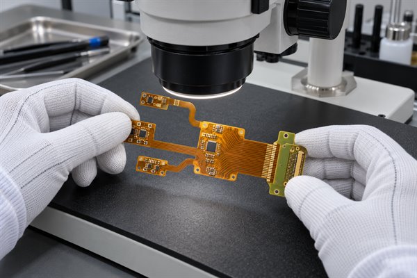
Project Background: BestFPC manufactured a 6-layer flexible PCB for a mobile phone application requiring multiple conductive layers within a compact structure. The board featured blind holes and separated flexible sections, accommodating complex electrical connections while maintaining flexibility in selected areas.
Requirements and Challenges: The project required a finished thickness of 0.40 ± 0.05 mm, excluding the stiffener, with 1/2 oz copper and a specified 50 Ω impedance. Its six-layer construction also incorporated blind-hole connections and separated flexible layers. The main challenge was accommodating the multilayer circuit within the required thickness while preserving the intended flexible sections.
BestFPC Solution: BestFPC fabricated the circuit using three double-layer flexible PCB sections, with separated layers between the second and third layers and between the fourth and fifth layers. A 0.48 mm FR4 stiffener reinforced the required area. The board also used ENIG surface treatment, white silkscreen, and 1/2 mil coverlay.
Project Results: BestFPC completed the documented 6-layer flexible PCB with blind holes, separated flexible sections, and an FR4 stiffener. The finished construction illustrates the manufacturing possibilities for compact multilayer circuits used in mobile communication equipment. The published project specifies a 50 Ω impedance target but does not include measured impedance or RF performance results.
What Information Should You Provide for an Accurate Telecom Flexible PCB Quote?
An accurate telecom flexible PCB board quotation requires complete fabrication files, electrical specifications, mechanical requirements, and order details. Missing material or stackup information can delay the review, particularly for controlled-impedance circuits.
-
PCB Files: Gerber files, drill files, board outlines, and fabrication drawings.
-
Board Specifications: Layer count, copper thickness, finished thickness, materials, stackup, and surface finish.
-
Electrical Requirements: Target impedance and tolerance, operating frequency, critical RF signal requirements, and electrical acceptance criteria.
-
Mechanical Requirements: Bend locations, bend radius, connector dimensions, stiffeners, and installation constraints.
-
Order Details: Prototype or production quantity, delivery destination, and required schedule.
For assembled boards, include the BOM, component placement data, and assembly drawings.
Send your files and specifications to sales@bestfpc.com. BestFPC can review the proposed construction, confirm applicable manufacturing capabilities, and prepare a project-specific quotation.
FAQs About Telecom Flexible PCB Boards
Q1: Can a flexible RF circuit replace a coaxial cable?
A1: Yes, in certain applications. An impedance-controlled flexible circuit can replace a short coaxial connection when insertion loss, shielding, connector transitions, and installation requirements are satisfied.
Q2: Can telecom flexible PCBs be supplied in panels for assembly?
A2: Yes. Flexible PCBs can be supplied in panels when the board outline, handling method, and assembly requirements permit. The panel layout, tooling features, and support method should be agreed upon before fabrication.
Q3: Can SMT components be mounted directly on a flexible PCB?
A3: Yes. Components can be assembled on suitable flexible PCB sections, often with local reinforcement. Components and solder joints should generally be kept away from areas intended for repeated bending.
Q4: Can multiple antenna elements share one flexible PCB?
A4: Yes. Multiple antenna elements can be integrated into one flexible circuit when sufficient space, isolation, and grounding arrangements are provided. Mutual coupling and antenna performance must be evaluated in the final equipment configuration.
Q5: Can a flexible PCB combine RF and control circuits?
A5: Yes. RF and control signals can share a flexible PCB when routing separation, reference conductors, grounding, and interference requirements are properly addressed.
Q6: Can a metal housing affect an FPC antenna?
A6: Yes. Nearby metal components can change antenna resonance, efficiency, and radiation patterns. Antenna performance should be checked in the final enclosure rather than only in an open test environment.
Q7: Is ENIG suitable for every FPC connector?
A7: No. ENIG is suitable for many solderable connections, but frequently mated contact fingers may require a specified hard-gold finish. The connector manufacturer's requirements should determine the surface treatment.
Q8: How should telecom flexible PCBs be packaged to prevent shipping damage?
A8: Flexible PCBs should be protected against uncontrolled bending, abrasion, contamination, and moisture exposure where applicable. Packaging should support the board shape, protect exposed contacts, and include ESD protection when required by the product.
Q9: Does electrical continuity testing confirm RF antenna performance?
A9: No. Continuity testing detects open and short circuits. RF performance may require impedance, return-loss, insertion-loss, radiation, or other measurements according to the device requirements.
Q10: Can approved prototype Gerber files be reused for production?
A10: Yes, provided the fabrication revision, materials, stackup, and acceptance requirements remain approved. Changes that affect electrical or mechanical performance should be reviewed before repeat production.
Conclusion: Custom Telecom Flexible PCB Manufacturing with BestFPC
A reliable telecom flexible PCB board must fit the available space while meeting the communication equipment's electrical and mechanical requirements. Choosing the right structure and material from the outset helps avoid unnecessary manufacturing complexity and reduces the risk of compatibility problems.
BestFPC provides custom telecom flexible PCB manufacturing backed by over 20 years of FPC experience, including DFM review, prototype fabrication, and volume production. Whether your project requires flexible antenna connections, multilayer FPCs, or rigid-flex circuits, send your Gerber files, specifications, and quantities to sales@bestfpc.com for a manufacturing review and custom quotation.


.png)
.png)
.png)
.png)

.png)