


 2026-11-05

 BEST
Rigid-flex PCB design for assembly requires careful control of component placement, bend geometry, solder pad support, and SMT handling. Poor decisions in these areas can cause cracked copper traces, lifted pads, solder defects, or interference when the finished board is folded into its enclosure.
The key is to design for both the flat SMT assembly process and the final folded configuration. These guidelines explain the design rules, calculations, and checks that help engineers identify assembly problems before production.

What Assembly Requirements Should Be Considered Before Rigid-Flex PCB Layout?
Define the final folded structure and assembly conditions before placing components. The rigid section positions, flex length, mounting surfaces, and folding sequence all depend on these requirements.
-
Final geometry: Record the position and orientation of each rigid section, mounting-hole locations, enclosure dimensions, and available folding space.
-
Bending duty: Distinguish between a flex section that bends during installation and one that moves repeatedly during operation.
-
Component mounting: Identify which rigid sections require single-sided or double-sided SMT assembly.
-
Mechanical loads: Locate connectors, fasteners, and other features that exert forces on the finished board.
-
Assembly sequence: Determine whether components will be mounted and tested before folding, and how the populated board will enter the enclosure.
For example, if two rigid sections must fold toward each other, the mechanical layout must show their separation, installed angle, and available bending space. Without these dimensions, the flex connection may be too short or require a radius smaller than the construction can tolerate.
How Should Rigid and Flexible Areas Be Arranged for Assembly?
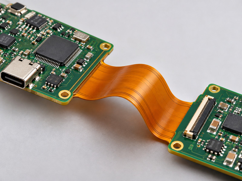
Place components and mounting features on rigid sections, and position flexible connections along the intended folding path. The arrangement must remain stable during SMT while allowing the populated board to reach its installed position without excessive strain.
-
Rigid-section dimensions: Allow enough space for components, connector loads, mounting holes, and assembly support.
-
Flex connection length: Include the required bending arc, straight portions, and mechanical tolerances. Do not determine the length from the distance between rigid sections alone.
-
Flex connection direction: Avoid layouts that require the flex to twist or stretch diagonally during installation.
-
Small rigid islands: Provide mounting or fixture support when a rigid section carries heavy components or connectors.
-
Assembly access: Ensure every populated rigid section can be reached by the placement equipment and inspected after soldering.
A short flex connection can pull against the rigid-to-flex boundary during installation. An excessively long connection may buckle or become trapped between enclosure parts.
If either condition occurs, change the rigid-section arrangement or flex path rather than forcing the board into place.
Where Should Components and Connectors Be Placed on a Rigid-Flex PCB?
BGA, QFN, large components, and mechanically loaded connectors should be mounted on stable rigid areas. Their bodies, solder pads, and load-bearing features must remain outside the approved bending and transition keepouts.
The placement requirements differ by component type:
-
BGA and QFN: Use sufficiently supported rigid areas and preserve access for soldering, inspection, and possible rework.
-
Board-to-board connectors: Provide a mechanical load path for insertion and removal forces. Avoid relying on narrow flex connections to hold the connector in position.
-
Heavy components: Keep them away from unsupported rigid edges and areas that can deflect during handling.
-
Flex-mounted SMT components: Restrict placement to approved non-bending areas with appropriate local reinforcement.
-
Fine-pitch connectors: Check mating clearance, adjacent component heights, and available assembly space.
Component-to-bend clearance cannot be defined by one universal distance. The required keepout depends on the rigid-to-flex structure, mounting method, and expected mechanical loads.
When reviewing placement, check the component body and solder pads separately. A component may be outside the bend while its solder joints remain too close to the transition.
Example: Connector Loading
A connector is mounted on a narrow rigid island connected to the main board by a flexible ribbon. During cable insertion, the island deflects and transfers force to the flex transition.
The correction is to provide mechanical support for the island or relocate the connector to a better-supported rigid area. Simply moving the connector a small distance from the transition may not resolve the loading problem.
What Are the Bend Area and Rigid-to-Flex Transition Design Guidelines?
The allowable bend radius depends on the finished flex construction, number of copper layers, bend direction, and expected movement. A radius suitable for a one-time installation bend may not be suitable for repeated bending.
The basic geometric relationship is:
R/t = Inside bend radius / Finished flex thickness
For example, a flex section with a finished thickness of 0.20 mm and an inside bend radius of 2.00 mm has an R/t ratio of 10:1.
This ratio describes the geometry. It does not establish the allowable bend radius or fatigue life of a specific construction.
How Can the Required Bend Length Be Calculated?
For a simple constant-radius bend, the approximate centerline arc length is:
L = θ × (R + t/2)
Where:
-
L: Centerline arc length of the curved portion.
-
θ: Bend angle in radians.
-
R: Inside bend radius.
-
t: Finished flex thickness.
For a 90° bend with R = 2.00 mm and t = 0.20 mm:
L = 1.571 × (2.00 + 0.10) ≈ 3.30 mm
The result covers only the curved portion. Straight sections, transition clearances, tolerances, and assembly allowances must be considered separately.
How Should the Bend Design Be Checked?
-
Static bends: Confirm the installed radius, forming method, and any additional movement during assembly or maintenance.
-
Dynamic bends: Specify the required cycle life and verify the complete flex construction for repeated movement.
-
Multilayer flex: Review the number and arrangement of bonded copper and dielectric layers, which affect bending stiffness.
-
Transition regions: Keep active bending away from abrupt stiffness changes, plated holes, solder joints, and other vulnerable structures.
For example, a 0.20 mm flex section with a proposed 2.00 mm radius may satisfy one construction's bending requirements but not another's. The actual stackup and bending duty must be checked before approving the geometry.
If the proposed radius is below the approved limit, increase the available bend space, change the mechanical arrangement, or revise the flex construction.
IPC-2223 provides relevant flexible and rigid-flex design guidance, but the final bend conditions must be verified for the specific construction.
How Should Traces, Vias, and Copper Be Designed to Withstand Assembly Stress?
Traces should cross active bends with smooth, consistent geometry. Vias, solder pads, and abrupt copper transitions should remain outside bending regions wherever possible.
-
Trace direction: Route traces approximately perpendicular to the bend line to reduce unnecessary strain along the conductor.
-
Trace transitions: Avoid sharp corners and abrupt width changes within active bends.
-
Vias: Keep plated holes in rigid or non-bending regions because their barrels are vulnerable to bending stress.
-
Multilayer routing: Stagger traces on different flex layers where possible to reduce local stiffness concentration.
-
Copper pours: Avoid unnecessary solid copper in active bends. Use alternative copper patterns only when electrical requirements permit.
-
Trace-to-pad connections: Keep vulnerable pad transitions away from locations subjected to repeated movement.
Example: Trace Damage Near a Transition
A trace crosses the flex section and makes a sharp 90° turn immediately beside the rigid edge. During folding, the change in board stiffness and conductor direction can concentrate strain in the same location.
Move the direction change into a non-bending area and route the conductor smoothly across the bend.
For dynamic applications, also verify the selected copper construction and routing against the required bending life. A trace that survives one fold may still fail after repeated cycles.
What Are the SMT Pad, Coverlay, and Solder Mask Design Guidelines?
SMT pad design must provide enough exposed copper for soldering while protecting the pad-to-trace connection from mechanical damage. Coverlay openings require particular attention because laminated coverlay generally has different alignment and minimum web-width limits from photoimageable solder mask.
-
Pad geometry: Use land patterns compatible with the component and soldering process.
-
Pad location: Keep solder joints outside active bending regions.
-
Pad anchoring: For components mounted on flex, consider suitable pad extensions and coverlay overlap where required by the construction.
-
Coverlay registration: Check opening dimensions against the fabricator's cutting and lamination tolerances.
-
Solder mask clearance: Ensure solder mask on rigid sections does not obstruct solderable pads or expose unwanted copper.
How Should Individual and Gang Openings Be Selected?
Individual openings are suitable when enough coverlay material remains between adjacent pads. A gang opening is often preferable when separate openings would create excessively narrow coverlay strips.
Consider an illustrative fine-pitch pad layout:
-
Pad pitch: 0.50 mm
-
Pad width: 0.25 mm
-
Proposed opening clearance: 0.10 mm on each side
-
Individual opening width: 0.45 mm
-
Remaining coverlay web: 0.50 − 0.45 = 0.05 mm
If the fabricator's minimum coverlay web exceeds 0.05 mm, the proposed individual openings are not acceptable.
One option is to use a shared opening across the pad group. However, this exposes the gaps between pads, so solder paste printing and solder bridging must be checked.
The pad anchoring arrangement also deserves attention. When multiple pads share one opening, appropriate extensions or coverlay anchoring features may be required to maintain mechanical reliability.
The values above illustrate the geometry calculation, not universal manufacturing limits.
An acceptable coverlay design must meet three conditions: sufficient solderable pad exposure, adequate insulation and anchoring, and an opening geometry compatible with the fabricator's process.
When Are Stiffeners Required for Rigid-Flex PCB Assembly?
Use stiffeners where non-bending flexible areas require additional support for components, connectors, or mechanical handling. A stiffener should solve a specific support problem without restricting the intended bending movement.
-
SMT components on flex: Add local reinforcement when the mounting area cannot remain sufficiently stable during soldering or operation.
-
ZIF connector tails: Match the final contact-tail thickness to the mating connector's specified requirements.
-
Through-hole connectors: Provide support for insertion forces and the intended soldering method.
-
Mechanically loaded areas: Reinforce flexible mounting locations that would otherwise deflect excessively.
FR-4 is commonly used where relatively rigid local support is required. Polyimide may be suitable for thinner or less rigid reinforcement.
For SMT components, a stiffener is often positioned on the opposite side of the mounting surface. The support area should extend sufficiently beneath the component and its solder joints, while remaining outside active bends.
The stiffener edge must also be checked. A stiffener ending inside a bend or immediately beside a vulnerable pad can concentrate strain.
For ZIF connectors, calculate the complete insertion thickness, including the flex construction, adhesive, protective layers, and stiffener. The stiffener thickness alone is not the connector mating thickness.
How Should Rigid-Flex PCBs Be Panelized and Supported for SMT Assembly?
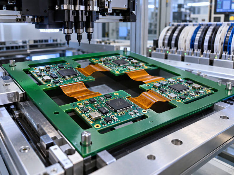
Every populated rigid section must remain stable during solder paste printing, placement, and reflow. Flexible connections cannot be assumed to provide adequate support for the attached rigid sections.
The assembly support requirements are:
-
Stencil printing: Support areas beneath solder paste locations must resist printing pressure without excessive board movement.
-
Component placement: Rigid sections must remain correctly positioned relative to fiducials during placement.
-
Reflow: The panel and carrier must be compatible with the intended thermal profile.
-
Depanelization: Board separation must not pull on flex connections or load nearby solder joints.
-
Fixture clearance: The carrier must avoid contact with components mounted on its supporting side.
Example: Solder Paste Defects Caused by Poor Support
Two rigid islands are connected by a narrow flex ribbon. The SMT panel holds the first island securely, but the second island has no backing support.
During stencil printing, the unsupported island moves under the printing load. Paste deposits may become misaligned or smeared, increasing the risk of solder bridging or insufficient solder.
The correction is to support both islands using an appropriate panel arrangement or carrier fixture. The carrier must hold the populated areas in the required plane while allowing safe removal after soldering.
Before production, confirm the location of tooling holes, fiducials, carrier support surfaces, and depanelization features with the assembly provider.
What Design Considerations Apply to Double-Sided SMT Assembly?
Double-sided SMT assembly requires support for the second side without damaging components already mounted on the first side.
-
First-side clearance: Ensure tall connectors and other mounted components do not interfere with the fixture when the board is turned over.
-
Second-side support: Reserve contact areas that will not press against existing components or unsupported flex regions.
-
Reflow retention: Evaluate large or heavy components that may shift during an inverted second reflow pass.
-
Thermal compatibility: Confirm that the board materials and components can tolerate the planned soldering cycles.
-
Assembly order: Select the mounting sequence that provides reliable soldering and fixture access.
For example, a tall connector on the first side may prevent the opposite surface from being properly supported.
Possible solutions include relocating the connector, changing its mounting side, designing a qualified fixture recess, or revising the assembly sequence.
If a stable second-side support method cannot be established, the component layout must be changed before production.
How Should Folding, Mechanical Clearance, and Final Assembly Be Planned?
Check the complete folding path using a populated 3D assembly model. A board that fits the final enclosure position may still collide with components during installation.
-
Folding clearance: Check rigid edges and component bodies at intermediate folding angles, not just at the final position.
-
Installed bend radius: Confirm the radius after mounting screws and brackets are secured.
-
Dimensional tolerances: Include PCB thickness, component height, mounting locations, and enclosure variation.
-
Connector engagement: Ensure cable insertion does not pull rigid sections away from their mounting positions.
-
Flex protection: Prevent the circuit from being pinched between enclosure parts or pressed against sharp edges.
Example: Interference During Folding
Two populated rigid sections are intended to fold to 90° inside an enclosure. The final positions appear correct in CAD, but a tall connector collides with a capacitor halfway through the folding movement.
The design can be corrected by relocating one component, changing the rigid-section arrangement, or revising the folding sequence.
Also check the installed configuration after fastening. If a screw shifts the rigid section and reduces the bend radius below the approved limit, the mounting arrangement must be revised.
How Should Test Points and Inspection Access Be Designed?
Test points should be located on supported rigid areas whenever possible. Electrical testing must not require excessive flexing or unsupported probe loading.
-
Test pads: Provide accessible locations and sufficient support for probe contact forces.
-
AOI: Preserve visibility of solder joints that require optical inspection.
-
X-ray: Account for inspection of hidden connections, including BGA solder joints.
-
Functional testing: Keep the necessary connectors accessible at the intended test stage.
-
Post-fold testing: Check electrical continuity or function in the installed configuration when bending can affect reliability.
If a PCB passes testing while flat but fails after folding, inspect conductors near the bend, rigid-to-flex transitions, solder joints, and connector interfaces.
This distinction is important because flat-board electrical testing alone may not reveal damage introduced during final installation.
What Assembly Drawings and Instructions Should Be Provided?
Provide separate fabrication and assembly information, with consistent dimensions and revision identifiers.
Fabrication files:
-
Gerber or ODB++: Copper, protective layers, drilling, and board outlines.
-
Stackup: Rigid and flexible materials, copper thicknesses, and finished thickness requirements.
-
Mechanical drawing: Rigid-to-flex boundaries, bend locations, directions, radii, and relevant tolerances.
-
Stiffener details: Material, thickness, position, adhesive requirements, and dimensions.
Assembly files:
-
BOM and Pick-and-Place: Component part numbers, coordinates, rotations, and mounting sides.
-
Assembly drawing: Component orientation, polarity, and special placement requirements.
-
Panel and fixture requirements: Tooling locations, fiducials, support conditions, and separation instructions.
-
Installation and test instructions: Folding sequence, final configuration, and required electrical or mechanical checks.
The flat PCB drawing and folded assembly drawing must describe the same approved design. Differences in bend positions, component placement, or rigid-to-flex boundaries can create assembly problems even when the electrical layout is correct.
Rigid-Flex PCB Design for Assembly Checklist
Use the following checklist before releasing fabrication and assembly files. A failed check requires a design correction or an approved technical disposition.
| Design Check | Acceptance Criteria | Corrective Action |
|---|---|---|
| Rigid-section arrangement | Fits the required assembly and installation geometry | Revise section locations |
| Flex length | Accommodates the bend arc, straight sections, and tolerances | Adjust the connection length |
| Component placement | Bodies and solder joints remain outside approved keepouts | Relocate components |
| Connector loading | Insertion forces have adequate mechanical support | Add support or move connectors |
| Bend radius | Meets approved construction-specific limits | Increase radius or revise construction |
| Bend life | Meets the defined bending-duty and qualification requirements | Reassess the flex construction |
| Trace and via layout | Meets the approved bend-region restrictions | Reroute traces or move vias |
| Coverlay openings | Pad exposure, registration, and web widths are acceptable | Revise the opening geometry |
| Pad support | Flex-mounted pads and components have adequate reinforcement | Add or modify support |
| Stiffeners | Provide support without interfering with active bends | Adjust stiffener geometry |
| SMT panelization | Populated areas remain stable during printing and placement | Revise panel or carrier |
| Double-sided SMT | Second-side processing clears mounted components and fixtures | Adjust layout or assembly sequence |
| Mechanical clearance | Full folding path and installed tolerances are acceptable | Revise PCB or enclosure |
| Inspection access | Test and inspection features remain accessible and supported | Relocate test points or modify access |
| Documentation | All fabrication and assembly files use the same revision | Correct inconsistent files |
A rigid-flex PCB is not ready for assembly simply because it passes electrical design checks. Bend limits, component support, SMT fixture compatibility, and final installation clearance must also be verified.
FAQs About Rigid-Flex PCB Design for Assembly
Q1: Does rigid-flex PCB assembly require special solder paste?
A1: Not necessarily. Conventional solder paste may be suitable when its alloy, flux chemistry, and reflow requirements are compatible with the PCB surface finish and components. Rigid-flex construction does not automatically require a different solder paste. The complete assembly should be qualified using the intended soldering process.
Q2: Is pre-baking required before rigid-flex PCB assembly?
A2: Pre-baking is not mandatory for every rigid-flex PCB. The decision depends on material construction, storage conditions, moisture exposure, and manufacturing recommendations. Excessive baking can also affect materials or dimensions. Use the fabricator's approved drying conditions rather than applying an arbitrary temperature and duration.
Q3: Can no-clean flux residues remain on flexible circuits?
A3: No-clean flux residues may be acceptable when the flux, soldering process, and final operating environment have been qualified. However, residues exposed to moisture or electrical bias may introduce reliability concerns. Residue acceptability should be established through the applicable cleanliness and reliability requirements, especially for high-impedance or moisture-sensitive applications.
Q4: Is ultrasonic cleaning suitable for assembled rigid-flex PCBs?
A4: Ultrasonic cleaning should not be selected without checking component compatibility and the mechanical characteristics of the assembly. Cavitation and vibration may damage sensitive components or unsupported structures. Use ultrasonic cleaning only when the equipment settings, cleaning chemistry, and complete assembly have been qualified.
Q5: Can rigid-flex PCBs be assembled using hand soldering?
A5: Yes. Hand soldering may be suitable for prototypes, low-volume assemblies, and selected components. The soldering area must be adequately supported, and heating must remain within the component and PCB material limits. Avoid pulling or bending flexible sections while solder joints are being formed or remain hot.
Q6: Can selective soldering be performed after SMT assembly?
A6: Yes, for suitable through-hole components mounted on supported rigid sections. The soldering equipment must have sufficient access, and nearby components and flexible materials must tolerate the process. Check nozzle clearance, local thermal exposure, and mechanical support before selecting selective soldering.
Q7: Is underfill necessary for every BGA mounted on a rigid-flex PCB?
A7: No. Underfill is application-dependent rather than a standard requirement for all rigid-flex PCB assemblies. It may improve mechanical reliability in certain environments but can complicate rework and introduce material compatibility concerns. Specify underfill only when package reliability requirements and qualification results justify its use.
Q8: Can conformal coating be applied after rigid-flex PCB assembly?
A8: Yes, when the coating is compatible with the PCB materials and operating environment. Connector contacts, test interfaces, and other areas requiring electrical access may need masking. Flexible regions also require a coating capable of accommodating their intended movement. Verify coating adhesion, thickness, flexibility, and masking requirements before application.
Q9: Which workmanship standards apply to assembled rigid-flex PCBs?
A9: IPC J-STD-001 establishes requirements for soldered electrical and electronic assemblies, while IPC-A-610 provides electronic assembly acceptability criteria. The applicable revisions and acceptance class should be agreed upon for the project. Bare-board requirements are addressed separately, including relevant flexible PCB specifications.
Q10: How should populated rigid-flex PCB assemblies be packaged before installation?
A10: Packaging should provide ESD protection and mechanical support appropriate to the assembled board. Trays or shaped supports can prevent unwanted movement, connector damage, and component compression. Avoid uncontrolled folding, stacking pressure, and unsupported rigid sections during handling and transportation.
Conclusion
Reliable rigid-flex PCB design for assembly requires correct component positioning, construction-specific bend limits, well-supported solder joints, stable SMT handling, and verified mechanical installation.
Before production, resolve any bend-radius violations, unsupported component areas, coverlay opening problems, or fixture interference identified by the checklist.
BestFPC manufactures custom rigid-flex PCBs according to customer-approved designs and material specifications. Submit your fabrication files, stackup requirements, quantity, target delivery date, and delivery location to request a manufacturing quotation.


.png)
.png)
.png)
.png)

.png)