


 2026-11-10

 BEST
PCB electrodes are conductive patterns formed on a circuit board to interact with a sensing material, sample, or electric field. For flexible sensors, the purchasing specification must define both the active surface and the circuit carrying its signal. Copper thickness, exposed area, surface finish, and the connection to the readout board all affect what should be manufactured.
At BestFPC, we combine custom flexible circuit manufacturing with PCB and PCBA engineering support for US sensor projects. Our DFM pre-review reports help resolve fabrication questions before production, while sample and small-batch support lets your team evaluate the electrode structure before scaling. Send your drawings and quantities to sales@bestfpc.com to discuss the board, surface finish, and assembly scope.
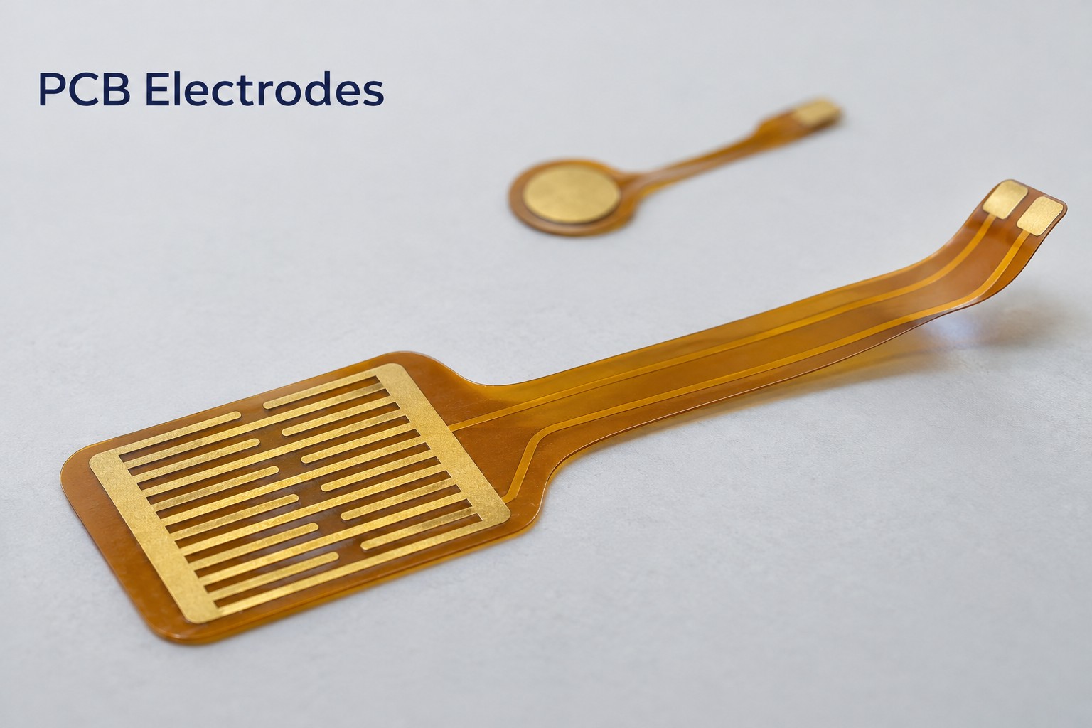
Custom PCB Electrodes for US Sensor Projects
We manufacture custom flexible circuits that can incorporate PCB electrode structures according to your drawings and agreed process requirements. The supply scope can include the patterned board, its connection tail, and separately specified assembly work.
The electrodes in a PCB may be the sensing interface, but they do not necessarily include the material that responds to pressure, humidity, or a chemical sample. Define that division before requesting a complete sensor assembly.
- Interdigitated patterns: Interdigitated electrodes, also called interdigital electrodes, use opposing fingers separated by gaps. For an interdigitated electrode sensor, specify which regions receive the sensing material and which remain insulated.
- Contact pads and arrays: Circular, rectangular, or repeated pads provide defined contact areas. Identify each pad's electrical net and mating surface so isolated channels are not unintentionally connected.
- Integrated flex tails: Flex PCB electrodes can extend into a flexible connection tail, avoiding a separate cable attachment at the sensing region. Tail length, routing, and the supported connection end belong on the same drawing.
Flexible PCB electrodes suit layouts that must conform to an enclosure or reach a nearby readout board. A flexible electrode PCB intended for repeated movement also needs a defined bend region and service conditions; a thin substrate alone does not establish its bending life.
Flexible PCB Electrode Manufacturing Capabilities
Our standard FPC capability includes 1–4 conductive layers and finished board thicknesses of 0.06–0.60 mm. Material and stiffener options below provide a starting point for a manufacturability review of your electrode layout.
| Construction Item | Standard Options |
|---|---|
| Conductive layers | 1–4 layers |
| Finished FPC thickness | 0.06–0.60 mm |
| Adhesive flex core | PI: 0.5, 1, 2 mil |
| Adhesiveless flex core | PI: 0.5, 1, 2, 3 mil |
| Copper, adhesive core | 0.33, 0.5, 1 oz |
| Copper, adhesiveless core | 0.33, 0.5, 1, 2 oz |
| PI stiffener | 3, 5, 7, 9 mil |
These are individual process options, not a guarantee that every listed minimum or maximum can be combined. Finished thickness depends on the selected copper, dielectric, adhesive, coverlay, and local reinforcement. For a thin electrode board, identify whether the thickness requirement applies to the active area, the flex tail, or the reinforced termination.
DFM for Flexible Electrode PCB Design
Our DFM review checks whether the electrode geometry, material stack, exposed areas, and outline can be manufactured together. The output should resolve drawing conflicts before tooling, rather than leave production staff to interpret the sensing area.
When you design copper electrodes on a PCB, define the following items in the fabrication package:
- Finished geometry: Give electrode width, spacing, active length, and acceptance tolerances. Our standard external line/space entry is 3.5/3.5 mil at 18 µm finished copper, before artwork compensation. This is a process reference for that copper condition, not a universal finished electrode-gap tolerance.
- Exposure boundaries: Dimension the openings around copper electrode pads and distinguish them from ordinary solder pads. A change in coverlay registration can change the exposed area even when the copper pattern remains unchanged.
- Copper near the outline: Mark intentionally exposed edges. A zero copper-to-edge requirement needs specific review of cutting, handling, and edge acceptance rather than being treated as a routine clearance.
- Moving and fixed regions: Locate bends away from reinforced transitions and identify the intended motion. Keep the sensing geometry and connection support requirements separate so reinforcement does not obstruct the active area.
For teams deciding how to design interdigitated electrodes in a PCB, the manufacturing drawing should specify finger count, overlap, gap, and the active-area opening. Manufacturing interdigitated electrodes on a PCB also requires agreement on which dimensions may be compensated during fabrication and which finished dimensions must be inspected.
An interdigitated electrode design is sometimes described as an interdigital electrode layout. Use consistent feature identifiers across the copper and coverlay files: changing finger spacing can change capacitance between electrodes, so a manufacturing adjustment affecting that spacing needs approval from the sensor designer.
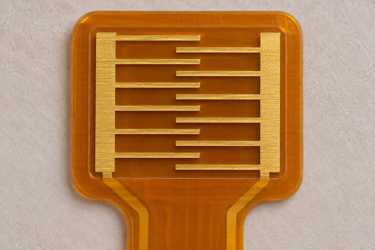
Gold Finishes and Exposed Copper for PCB Electrodes
Our FPC process options include immersion gold and electroplated gold; the choice must match the electrode's operating environment and connection requirements. For a flexible PCB board design with gold electrodes, specify the coating system, layer thicknesses, and active area rather than requesting only a “gold finish.”
A PCB finish used successfully for soldering is not automatically suitable for prolonged contact with an electrolyte. For liquid-contact electrodes, provide the sample chemistry, exposure duration, and electrical operating conditions so the finish requirements can be reviewed against the application.
- Separate sensing and soldering zones: Identify pads that must accept solder independently of the active electrode surface. A hard-gold request should include the intended gold type and thickness; its compatibility with the assembly process and the plating connection arrangement need review.
- Define acceptable bare-copper condition: Copper PCB electrodes supplied without a protective finish need an agreed surface acceptance condition. Specify whether discoloration is acceptable and how boards will be stored and prepared before use.
- Protect areas outside the electrode: Retain insulation over routing where the design permits. This helps define the exposed surface without unnecessarily exposing unrelated conductors to the sample or handling.
PCB Electrode Connections and Assembly Options
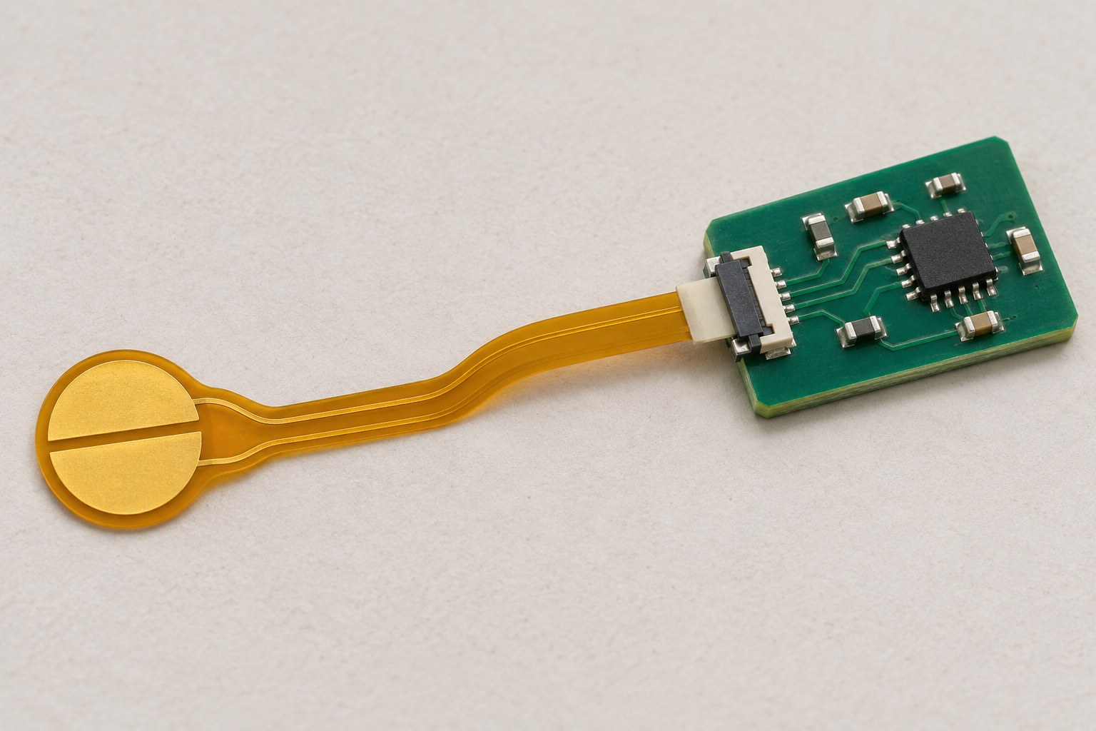
Electrode boards can connect to a readout circuit through soldered leads, a connector-compatible flex tail, or an assembled interface. Choosing how to connect electrodes to a PCB starts with the mating connection and mechanical loads, not just the available pad area.
- Soldered leads: Specify wire size, pad geometry, and attachment direction. Add mechanical support so movement of the wire is not transferred directly into the thin copper pad.
- Flex-tail connectors: Supply the connector part number and its required contact orientation, pitch, and insertion thickness. Stiffener thickness alone is insufficient because adhesive and the underlying FPC also contribute to the mating thickness.
- Board-level assembly: Our PCB manufacturing, component procurement, and PCBA services can support an agreed interface assembly. Provide the BOM, placement data, and test requirements so component sourcing and assembly suitability can be reviewed together.
Keep flux, solder, and cleaning processes away from sensitive exposed regions unless the sensor design allows them. For assemblies needing a clean active surface, specify the process sequence and surface acceptance requirements before components are attached.
Inspection and Acceptance Criteria for PCB Electrodes
Acceptance should cover the manufactured circuit and its exposed surface, with sensor performance assessed against a separate application test plan. Define the inspection scope and required records in the order so dimensional approval is not mistaken for sensor qualification.
- Dimensions and exposed area: Specify finished electrode width and gap tolerances, plus coverlay registration limits. Measure the exposed area against the approved drawing; checking the copper pattern alone does not confirm the opening.
- Electrical connections: Use the approved netlist to define intended connections and isolated channels. Agree the continuity and isolation test limits before production.
- Surface and coating: Define acceptable residue, damage, and oxidation, along with the required coating thickness and supporting inspection records. Use agreed defect criteria rather than a general requirement for a “good surface.”
The chosen measurement method, sampling plan, and deliverable records should be agreed before production. This is particularly important when the active area has tighter acceptance requirements than the rest of the circuit.
For development work, retain the board revision and sample-lot identity with the sensor test results. Our digital production traceability supports tracking material and product batches, helping teams investigate whether a later issue relates to a design change or a production lot. Electrical continuity checks alone do not establish electrochemical stability, biocompatibility, or measurement accuracy.
PCB Electrode Prototypes, Pricing, and Production Orders
We support samples and small batches for electrode evaluation before production quantities are released. Pricing depends on board construction, plated area, panel utilization, special processing, and inspection scope; lead time must be confirmed for the selected build and material availability.
- Submit one consistent design revision. Include Gerber data, the stack-up, finish requirements, and exposure drawings. Add quantities and the intended operating environment so the quotation covers the required construction rather than an assumed standard finish.
- Resolve fabrication questions. Our PCB and PCBA engineers provide DFM analysis and process-adaptation advice. For assembled versions, a BOM optimization list can identify component or sourcing questions before purchasing begins.
- Evaluate the sample build. Check the board in the intended sensing setup, including the final connection and any added sensing layer. Record the accepted construction and test conditions before increasing the order quantity.
- Release the production specification. Freeze the drawings, agreed finish, acceptance criteria, and packaging requirements. For US deliveries, confirm the receiving address, shipping terms, and documentation requirements alongside the production schedule.
Compare quotations against the same active area, surface specification, and inspection scope. A lower board price based on a different finish or relaxed gap requirement may not represent an interchangeable electrode.
FAQs about PCB Electrodes
Does an electrode board include the sensing material?
Only if it is explicitly included in the supply scope. A patterned electrode board may require a separate pressure-sensitive film, functional coating, or other sensing material before it can perform the intended measurement.
Can I order a flexible board with all coverlay removed?
Submit it for a specific construction review. Removing all coverlay changes insulation, handling, and conductor exposure across the board; it is not simply a larger opening around the sensing pads.
How should I compare gold versus silver PCB electrodes?
Compare the electrode's role and operating chemistry first. A gold working electrode and a silver/silver-chloride reference electrode serve different functions; they are not interchangeable finish choices. Define the required electrode system before requesting a manufacturing quotation.
Are etched copper electrodes and printed electrodes the same?
No. Etched electrodes are patterned from copper foil, while printed electrodes are formed by depositing conductive ink or paste. Their materials and processing requirements differ, so specify the required construction instead of using “printed circuit” to imply an ink-based electrode process.
Can a finish change use the previous sample approval?
Do not assume so. Changing the finish can change the sensing interface even when the copper artwork stays the same. Review the change with the sensor designer and determine which application tests must be repeated.
Are these boards manufactured in the USA?
We are a China-based manufacturer supplying US projects. Confirm the manufacturing and assembly scope, shipping arrangements, and receiving requirements when placing the order.
Our engineering support includes DFM pre-review reports to turn electrode drawings into clear fabrication requirements. With our own PCB and PCBA factories and sample-to-small-batch support, we can coordinate the board and agreed interface assembly while your team evaluates the sensing system. Send your layout, surface requirements, and quantities to sales@bestfpc.com for a project-specific manufacturing review.


.png)
.png)
.png)
.png)

.png)