


 2026-11-10

 BEST
A hard gold PCB uses an electroplated gold alloy finish on specified conductive areas, typically where repeated contact or sliding wear makes the surface finish important. A successful build must also account for the board structure, mating interface, and soldering requirements.
At BestFPC, we combine flex and rigid-flex fabrication, manufacturing design review, and PCB assembly support for projects with demanding contact requirements. Our hard gold finger and selective gold plating services help you define the contact areas within a manufacturable circuit. Send your drawings and application requirements to sales@bestfpc.com to discuss a suitable build.
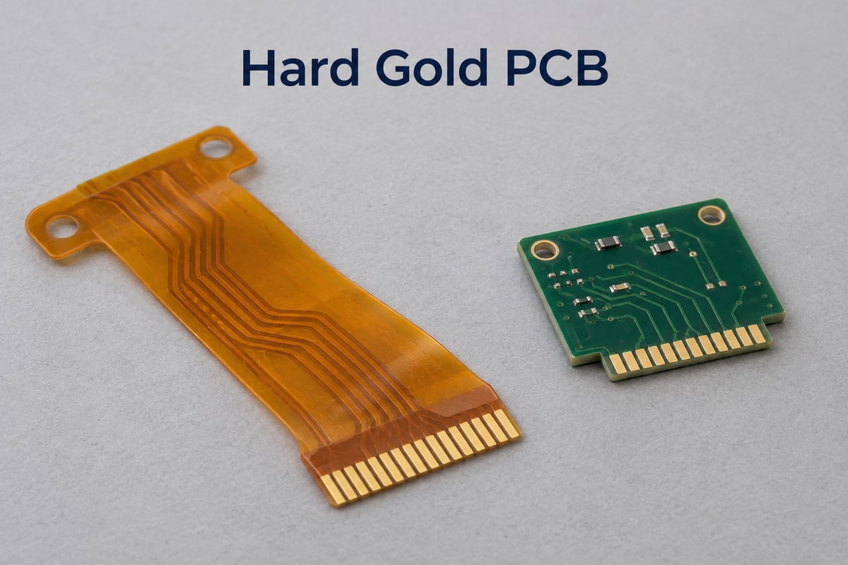
Custom Hard Gold PCB Types Available from BestFPC
We manufacture custom flexible and rigid-flex circuits, with hard gold contact requirements reviewed against the selected construction. The starting point is the board structure and connection arrangement, not simply the presence of a gold-colored surface.
| Board Type | Typical Applications | Potential Hard Gold Contact Area |
|---|---|---|
| Single-sided flex | Keypad and control-panel interconnects | Connector-tail fingers |
| Double-sided flex | Handheld instrument and sensor-module interconnects | Exposed connector contacts |
| Multilayer flex | Imaging-module and compact electronics interconnects | Reinforced terminal fingers |
| Rigid-flex | Plug-in controller and equipment modules | Rigid-edge connector fingers |
These applications illustrate suitable construction choices. The required finish depends on the mating interface and contact duty; not every circuit in these applications requires hard gold.
A PCB with hard gold finger contacts may use a reinforced flex tail or an appropriate rigid board edge. The mating gold finger connector determines the required contact geometry and finished insertion thickness. Adding a stiffener to an FPC does not, by itself, make it a rigid-flex PCB.
For a gold-plated PCB board, specify whether the gold serves as a wear surface, a solderable finish, or another functional surface. Hard gold plating on a PCB board must be selected for that function; it is not interchangeable with every other gold finish.
BestFPC’s Expertise in Surface Finishes for Flex and Rigid-Flex PCBs
We offer hard gold and ENIG finishes for flexible and rigid-flex circuits, with plating specifications matched to the contact and assembly requirements. The gold-finish options below give your engineers a clear starting point for specifying the plated layers.
| Finish Option | Gold Thickness | Nickel Thickness | Application Focus |
|---|---|---|---|
| Selective hard gold — 30 µin | 30 µin / 0.762 µm | 100 µin / 2.54 µm | Specified connector fingers and contact pads |
| Selective hard gold — 50 µin | 50 µin / 1.27 µm | 100 µin / 2.54 µm | Contacts requiring a thicker gold deposit |
| ENIG | 0.05–0.10 µm | 3–6 µm | Solderable component pads |
These are specification options, not interchangeable grades. The fabrication drawing should identify the plated areas and state whether the thickness values are minimum requirements or nominal targets. We confirm the selected combination against the board construction before production.
A hard gold PCB finish is intended for suitable wear-contact applications, while solder pads may need a different finish. When comparing ENIG vs. hard gold for a PCB, consider how the surface will be used. ENIG provides a thin immersion-gold layer over electroless nickel; it should not automatically replace a specified wear-resistant hard gold deposit.
We also offer OSP and tin plating, with ENEPIG available following special-process review. For boards combining hard gold contacts with solderable areas, we review the finish boundaries and processing sequence to coordinate both requirements within the manufacturing route.
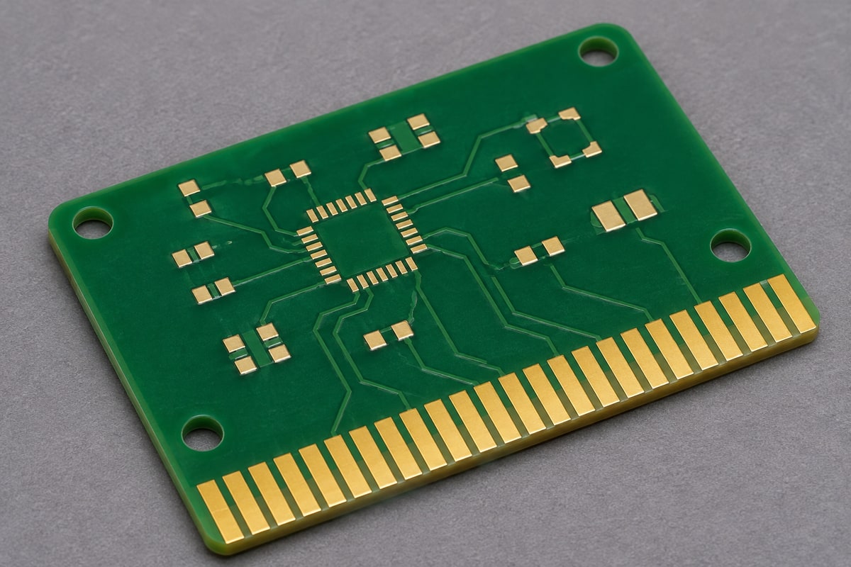
Custom PCB Hard Gold Plating Specifications
Our PCB hard gold plating specifications are established from the required deposit, plated area, and acceptance criteria. The fabrication drawing should distinguish hard gold chemistry from selective plating coverage: “hard” describes the deposit, while “selective” describes where it is applied.
For selective hard gold plating on a PCB, define:
- Plated area: Identify the fingers, pads, or electrode surfaces requiring treatment, including both sides where applicable.
- Gold and nickel layers: State each required thickness separately, with the measurement unit and whether the value is a minimum or nominal target.
- Deposit requirements: Include any applicable hardness, composition, or customer finish specification.
- Measurement locations: Identify the functional surfaces where the stated requirements must be met.
PCB hard gold plating thickness must be unambiguous. For example, a drawing requirement of 30 µin converts to 0.762 µm; this is a unit conversion, not a universal thickness recommendation or a stated manufacturing limit.
Requests for thick gold PCB fabrication also need a defined deposit and application. “Thick gold” alone does not establish hardness, wear performance, or the correct PCB gold plating process. We review the hard gold plating process for the PCB against the approved drawing before releasing the build.
DFM Support for Gold Fingers and Flex Connector Tails
Our DFM support focuses on whether the contact structure can be manufactured and will match the specified mechanical interface. For a fine-pitch PCB with selective hard gold, plating access and dimensional tolerances must be considered alongside trace routing.
- Plating connections: Review the temporary conductive paths needed for electroplating and how they will be removed or isolated without affecting the final circuit.
- Contact geometry: Check finger width, spacing, exposed length, and position against the mating connector drawing.
- Tail reinforcement: Evaluate the complete insertion stack, including the circuit, adhesive, and stiffener. Stiffener material thickness alone is not the finished tail thickness.
- Coverlay and bend transitions: Position openings and reinforcement so they support the contact region without placing an abrupt stiffness change in a required bend.
For hard gold edge connectors on PCBs, beveling requirements apply to the appropriate rigid edge geometry. Flexible connector tails require their own insertion and reinforcement review; the same edge treatment cannot be assumed for both.
Hard Gold PCB Assembly Services
We offer FPC and rigid-flex assembly support, including SMT and suitable mixed-technology builds. For boards with hard gold contacts, the assembly plan must keep the mating surfaces clean and free from solder or coating where those materials would interfere with contact.
- Assembly support: Plan carriers, panel handling, and local support so flexible areas remain stable during component placement and soldering.
- Soldering protection: Keep non-soldering fingers outside the intended solder contact area. Where wave soldering is involved, assess suitable shielding or selective processing for the board geometry.
- Cleaning and coating: Define contact keep-out areas and compatible cleaning requirements so residues or protective coatings do not obstruct the connection.
Hard gold edge contacts and wave soldering are separate design considerations: one concerns the mating surface, the other the assembly process. Identifying both in the assembly instructions helps prevent the contact finish from being treated as an ordinary solder pad.
Quality Control for Hard Gold PCB Orders
Our quality control includes incoming inspection, in-process checks, and board inspection and electrical testing before delivery. Hard gold orders also need finish-specific acceptance requirements agreed for the actual plated areas.
| Inspection Area | Acceptance Basis | Risk Addressed |
|---|---|---|
| Contact surface | Agreed appearance criteria | Damage or contamination |
| Contact and tail dimensions | Approved mechanical drawing | Connector mismatch |
| Circuit continuity and isolation | Released electrical data | Opens and shorts |
| Plated layers | Agreed thickness and deposit requirements | Incorrect contact finish |
Where thickness reports or other plating evidence are required, agree on the measurement method, locations, and reporting scope before production. A visual inspection cannot establish coating thickness.
Mating-cycle or contact-resistance qualification is a separate requirement. It needs defined mating hardware, loading, environment, and pass/fail criteria; a bare-board electrical test does not establish connector service life.
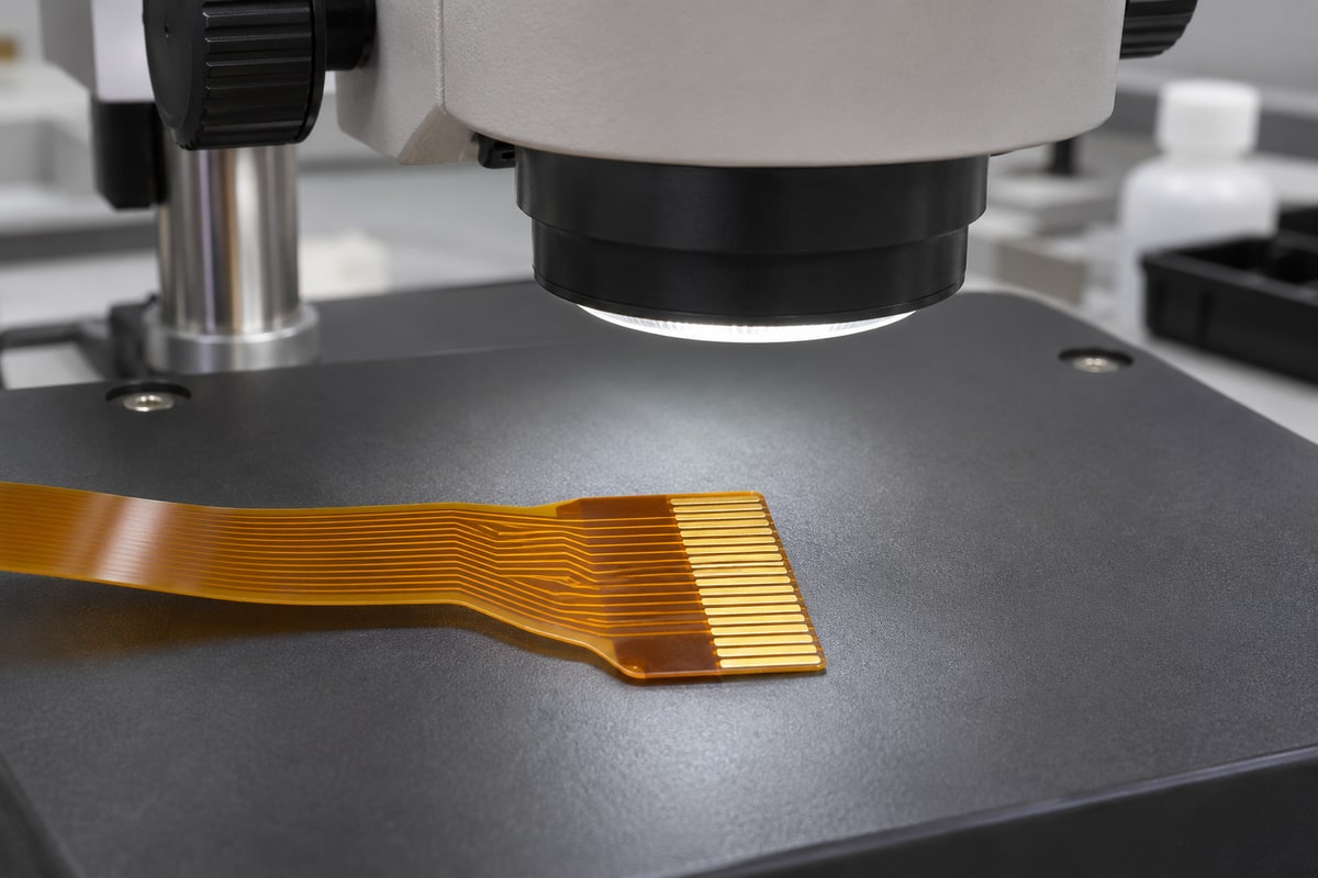
Hard Gold PCB Case Study
A four-layer USB-to-UART interface board shows how selective hard gold can be combined with a solderable finish on a compact plug-in PCB. This rigid-board construction suits a host-controller interface that needs durable edge contacts and soldered components on the same board.
The design uses ENIG for the solderable areas and a separate hard gold specification for the edge fingers. Its manufacturing requirements are:
| Parameter | Specification |
|---|---|
| Construction | Four-layer FR-4, Tg170 |
| Finished thickness | 0.8 ± 0.1 mm |
| Copper | 1 oz, inner and outer layers |
| Solderable finish | ENIG, gold 2 µin |
| Finger finish | Hard gold, nickel 100 µin / gold 50 µin |
| Edge bevel | 45°, per approved drawing |
| Outline tolerance | ±5 mil |
Manufacturing challenges and solutions
- Two finishes on one board: Keep the finger treatment separate from the ENIG regions in the production artwork. This preserves the specified contact deposit while providing the intended solderable surfaces.
- Mechanical fit at the interface: Control the finished board thickness, outline, and bevel together. A correctly plated finger still needs the right geometry to enter and seat in its mating connector.
- Impedance-sensitive routing: Confirm the stackup and production files before fabrication, preserving the impedance requirements alongside the contact geometry.
Customer value
The construction addresses soldering and edge-contact requirements within one board, while the drawing approval step brings finish boundaries, mechanical fit, and stackup into the same manufacturing review. These are the specifications of this rigid-board design; a flex or rigid-flex version needs its own construction review.
Hard Gold PCB Lead Times
Hard gold PCB lead times are confirmed for the reviewed construction, finish requirements, and order quantity. A standard flex-board turnaround should not be assumed to cover additional plating operations, special materials, assembly, or qualification work.
Plan the schedule around three milestones:
- Engineering release: Resolve drawing conflicts and approve the stackup, finish callout, and manufacturing changes.
- Manufacturing and inspection: Allow for material availability, the required process route, and any agreed additional measurements.
- Assembly and dispatch: Include component availability and assembly testing where applicable, then distinguish dispatch from delivery at your destination.
For a new design, leave time for sample evaluation before committing the production batch. For a repeat order, identify any changed files or specifications before requesting the same schedule as the previous build.
Hard Gold PCB Cost Optimization
Hard gold PCB cost optimization starts with controlling plated area and avoiding specifications that exceed the functional need. Savings should come from an agreed manufacturing change, not from silently reducing a required contact finish.
- Limit coverage to functional areas: Selective plating can reduce gold consumption, although masking and extra processing must be included in the comparison.
- Specify thickness for the application: Increasing thickness increases deposited gold, but does not by itself guarantee a proportional increase in useful life.
- Review panel use: Board outline, tooling space, and plating connections affect how efficiently the design can be processed.
- Compare realistic quantities: For bulk hard gold PCB orders, compare the total purchasing plan, including setup allocation, inventory needs, and the risk of a later design revision.
The best option is the lowest-cost construction that still meets the approved performance and acceptance requirements. Changes to material, finish, or geometry should remain visible in the quotation and drawing revision.
How to Request Hard Gold PCB Quotes
To request hard gold PCB quotes, send a consistent set of manufacturing files and identify whether you need bare boards or assembled units. A project-specific quotation is more useful than a general hard gold PCB price list from China because the supplied scope must match your design.
Please include:
- Fabrication data: Gerber files, drill data, stackup, and fabrication drawing with the finish callout.
- Mechanical requirements: Board outline, contact dimensions, stiffener details, and mating connector information where relevant.
- Order details: Prototype and production quantities, required delivery date, and destination.
- Acceptance requirements: Inspection criteria and any requested reports or special tests.
- Assembly data, if needed: BOM, placement file, assembly drawing, and test requirements.
Use the same revision across all files and identify any open technical questions. Send the package to sales@bestfpc.com so we can review the required supply scope and prepare the quotation.
Why Choose BestFPC as Your Hard Gold PCB Supplier?
We support hard gold PCB projects with certified quality systems, experienced engineering teams, and integrated PCB and PCBA manufacturing in China. For buyers comparing hard gold PCB suppliers, these resources connect technical decisions with material sourcing, production control, and delivery planning.
- Certified Quality Systems: Our ISO 9001, ISO 13485, IATF 16949, and AS9100D certifications support supplier qualification and quality management for industrial, medical, automotive, and aerospace projects within their applicable scopes.
- Experienced engineers with practical review deliverables: Our R&D and PCB/PCBA engineering team includes engineers with 20 years of experience. We provide DFM pre-review reports, process-adaptation recommendations, and BOM optimization lists for assembly projects, helping your engineers resolve contact geometry, material compatibility, and component-selection issues before production.
- Owned PCB and PCBA factories with integrated sourcing: We combine board manufacturing, component procurement, assembly, and testing, supported by more than 1,000 supply-chain partners. This gives your project a coordinated supply route and helps align material availability with production and quality requirements.
- Prototype and small-batch support: We support engineering samples and low-volume builds so you can evaluate connector fit, assembly compatibility, and the required contact performance before committing to a larger order.
- Digital production traceability: Our digital workshop enables material and product batch information, production-cycle records, and production progress to be retrieved within five seconds. This supports prompt investigation of material or batch questions and clearer project-status communication.
- Fast PCBA delivery: We offer a 1.5-week fast-delivery option for eligible PCBA projects, subject to component availability, approved technical files, and the agreed process route. Hard gold fabrication and additional qualification requirements are assessed separately when confirming the complete order schedule.
As an expert hard gold PCB supplier in China, we bring engineering review, factory production, and assembly resources together to help your team move from a defined contact requirement to a build ready for evaluation.
FAQs about Hard Gold PCB
Does every gold finger require hard gold?
No. The finish depends on contact motion, mating frequency, contact force, and the connector specification. A gold-colored contact is not sufficient evidence that a particular deposit is suitable.
Does thicker hard gold guarantee more mating cycles?
No. Wear also depends on contact geometry, loading, the mating material, and the operating environment. Cycle-life claims need testing under defined conditions.
Is hard gold suitable for wire bonding?
Do not assume that a wear-contact finish is suitable for wire bonding. The bonding process may require a different gold purity or finish system; specify the bonding method and obtain a compatible surface recommendation.
BestFPC offers custom flex and rigid-flex fabrication, hard gold finger options, and assembly support to help turn your contact requirements into a coordinated board build. We can review the contact structure alongside reinforcement and assembly needs, helping you identify manufacturing issues before ordering. Send your drawings and quantities to sales@bestfpc.com to discuss your project.


.png)
.png)
.png)
.png)

.png)