


 2026-11-19

 BEST
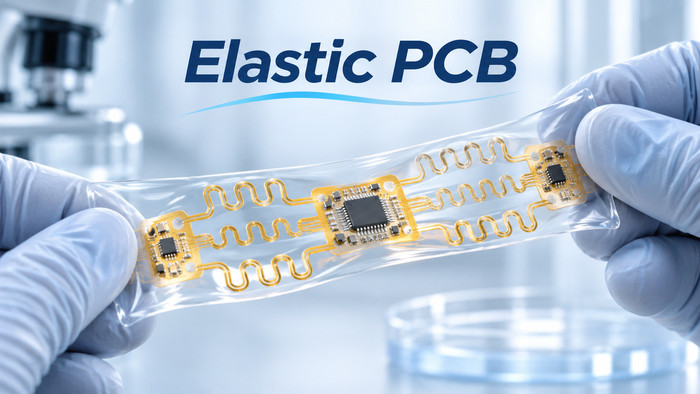
An elastic PCB, also known as a stretchable PCB, is a circuit designed to maintain electrical connections during stretching, twisting, and mechanical deformation. Unlike conventional flexible PCBs, which primarily bend or fold, elastic PCBs use elastomeric substrates and specially engineered conductive structures to accommodate tensile strain. They are used in medical skin patches, wearable health monitors, and soft electronic devices.
Are you dealing with broken conductive traces, unstable resistance, or damaged component connections caused by repeated stretching? These failures often result from unsuitable materials, conductor geometry, or concentrated mechanical stress. However, not every wearable device requires a stretchable circuit. Understanding elastic PCB structures, materials, applications, and their differences from flexible PCBs can help you select a more suitable solution without introducing unnecessary manufacturing complexity.
What Is an Elastic PCB and How Does It Work?
An elastic PCB is a printed circuit designed to maintain electrical continuity within a specified range of tensile deformation. It is also called a Stretchable Printed Circuit (SPC), Elastic Circuit, or Stretch Circuit.
Conventional flexible PCBs can bend, but their copper traces and insulating substrates are generally unsuitable for significant repeated stretching. Elastic PCBs accommodate deformation through two main mechanisms:
-
Material Stretchability: Elastomeric substrates such as thermoplastic polyurethane (TPU) and polydimethylsiloxane (PDMS) can stretch and recover. When combined with suitable stretchable conductive materials, they allow certain circuit regions to deform with the substrate.
-
Geometric Deformation: Serpentine, meander, and horseshoe-shaped traces absorb displacement through bending, rotation, and geometric extension, reducing the tensile strain experienced by the metal conductor itself.
For example, if a 100 mm circuit section is extended to 110 mm, its overall engineering strain is 10%. With properly designed serpentine interconnects, some of this displacement can be absorbed by changes in trace geometry rather than requiring the copper itself to elongate by 10%.
After the external force is removed, the substrate can recover toward its original shape. However, the circuit must also remain electrically functional. Conductor fatigue, damaged interfaces, or permanent resistance changes can occur even when the substrate appears to recover normally. Mechanical recovery and electrical continuity must therefore be evaluated together.
What Are the Main Structures of an Elastic PCB?
Elastic PCBs generally use two structural approaches: fully stretchable structures and island-bridge structures. The main difference is how each design distributes mechanical strain and protects electronic components.
1. Fully Stretchable Structure
A fully stretchable structure combines an elastomeric substrate with conductive networks and functional materials designed to deform within a specified strain range.
Its main structural elements include:
-
Elastomeric Substrate: TPU, PDMS, or other elastomers provide mechanical support and shape recovery.
-
Stretchable Conductive Network: Conductive composites, specially engineered metal interconnects, or liquid-metal channels maintain electrical connections during deformation.
-
Compliant Functional Layers: Suitable sensing or electronic materials allow functional regions to deform with the surrounding substrate.
-
Elastic Encapsulation: Protective layers shield conductors from mechanical damage and environmental exposure while preserving the required flexibility.
This structure is suitable for large-area strain sensors, skin-mounted electrodes, and soft electronic devices. When conventional rigid ICs are incorporated, additional strain isolation is generally necessary to prevent mechanical damage to the components.
2. Island-Bridge Structure
An island-bridge structure separates relatively rigid component mounting areas from deformable interconnections. Electronic components are positioned on stable islands, while stretchable bridges accommodate movement between them.
-
Rigid Islands: Provide stable mounting areas for ICs, sensors, and other electronic components.
-
Stretchable Bridges: Use serpentine or other compliant conductor geometries to accommodate displacement between adjacent islands.
-
Strain-Relief Regions: Reduce mechanical stress at transitions between rigid component areas and soft substrates.
-
Island Layout: Controls the spacing and arrangement of component regions according to the expected stretching direction, displacement, and device dimensions.
Island-bridge structures are particularly useful for wearable electronic systems that integrate conventional semiconductor components. By directing most deformation into the connecting bridges, the structure reduces tensile loading on component packages and electrical joints.
Serpentine traces can also be used within island-bridge structures. They are a conductor geometry rather than a separate structural category.
Which Materials Are Used in Elastic PCB Manufacturing?
Elastic PCB manufacturing involves elastomeric substrates, conductive materials, and protective encapsulation layers. Material selection affects stretchability, electrical stability, processing temperature, adhesion, and long-term durability.
| Material | Main Function | Properties and Limitations |
|---|---|---|
| TPU | Elastic substrate | Available as thin films; suitable for certain printed circuits; processing temperature and adhesion require attention |
| PDMS | Substrate, encapsulation | Soft and conformable; surface treatment and conductor adhesion can be challenging |
| Ecoflex | Soft substrate, encapsulation | Low stiffness and suitable for soft sensors; dimensional stability and structural support require consideration |
| Copper | Metallic interconnects | High conductivity but limited intrinsic stretchability; requires suitable geometric design |
| Silver-based conductive ink | Printed conductive traces | Stretchable formulations are available; resistance changes, adhesion, and cyclic durability must be evaluated |
| Liquid metal | Specialized stretchable interconnects | Can maintain conductivity under substantial deformation; encapsulation, leakage, and connection methods require control |
Material selection also depends on the intended application. Skin-mounted sensors often prioritize softness, skin-contact safety, and signal stability. Smart textiles must account for movement, perspiration, and washing, while high-density electronic assemblies require additional consideration of conductor patterning and component attachment.
No single material provides maximum stretchability, minimum electrical resistance, and the simplest manufacturing process simultaneously. The complete material system should be selected according to allowable resistance changes, mechanical lifetime, operating temperature, and environmental conditions rather than substrate elongation alone.
What Are the Main Applications of Elastic PCBs?
Elastic PCBs are used where circuits must stretch with the human body, textiles, or other deformable structures. Their main applications include:
-
Medical Skin Patches: ECG, EMG, and other physiological monitoring patches must accommodate skin movement. Stretchable circuits help reduce mechanical pulling on electrodes and connections while maintaining the required signal performance.
-
Wearable Health Monitoring: Respiratory monitoring, muscle activity detection, and motion tracking systems may require circuits that follow repeated movement around the chest, joints, or muscles.
-
Smart Textiles: Stretchable conductive networks can connect distributed sensors embedded in clothing for posture monitoring, activity tracking, and interactive garments.
-
Electronic Skin and Soft Sensors: Flexible sensing networks can integrate strain, pressure, and tactile sensors across curved or deformable surfaces.
-
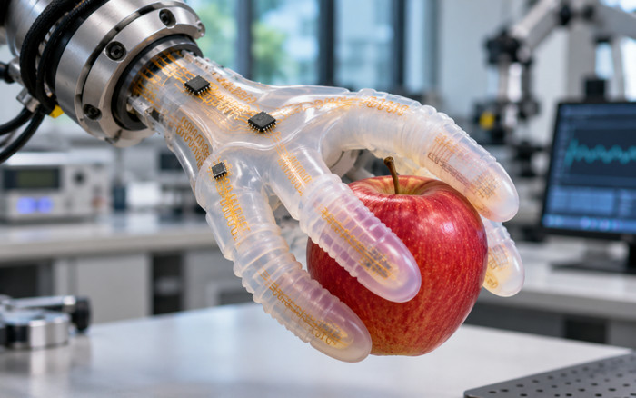
Soft Robotics: Stretchable interconnects connect sensors and functional elements across soft actuators and robotic structures that undergo extension, bending, or twisting.
Each application introduces different reliability requirements. Medical patches emphasize electrode contact, stable signal acquisition, and material safety. Smart textiles must also withstand friction and moisture exposure, while soft robotics may involve larger displacements and multidirectional deformation.
The intended application determines the mechanical strain, electrical performance, and reliability tests required for an elastic PCB.
What Are the Advantages of Elastic PCBs?
The main advantage of an elastic PCB is its ability to accommodate mechanical deformation while maintaining electrical functionality.
-
Stretching and Twisting Capability: Properly designed substrates and interconnects can withstand specified deformation, making them suitable for electronic systems that move continuously.
-
Improved Surface Conformity: Soft materials follow body contours and irregular surfaces more closely, reducing the mechanical restrictions associated with rigid circuit structures.
-
Reduced Interconnection Stress: Compliant conductors absorb relative movement between circuit regions, potentially reducing reliance on separate wires or moving connectors in certain applications.
-
Distributed Sensor Integration: Stretchable networks allow multiple sensing elements to be positioned across deformable surfaces while maintaining their electrical connections.
These advantages do not mean elastic PCBs are necessarily thinner, less expensive, or more durable than conventional flexible PCBs.
Their primary benefit is maintaining circuit functionality under specified stretching conditions, not simply allowing a circuit board to bend.
What Are the Limitations and Reliability Challenges of Elastic PCBs?
The main reliability challenges of elastic PCBs include conductor fatigue, resistance drift, component connection failures, delamination, and limited cyclic durability. Each failure mechanism requires appropriate design controls and verification.
1. Conductor Fatigue and Trace Cracking
Repeated stretching can concentrate mechanical stress around serpentine bends, conductor defects, and transitions between materials with different stiffness.
-
Design Considerations: Optimize trace curvature, width, conductor thickness, and transition geometry to reduce localized strain.
-
Verification: Perform cyclic stretching at the specified strain while monitoring electrical resistance and inspecting traces for cracking.
2. Resistance Drift and Signal Instability
Stretching can change conductor geometry or the contact between conductive particles, affecting electrical resistance. In signal-sensitive sensors, these changes may introduce measurement errors.
-
Design Considerations: Select conductors with suitable electrical stability and optimize interconnect geometry for the required current or signal characteristics.
-
Verification: Record resistance before stretching, during extension, and after recovery to distinguish reversible changes from permanent degradation.
3. Component and Connection Failures
Conventional semiconductor packages and solder joints are much stiffer than elastomeric substrates. If placed in high-strain regions, their connections may crack or separate during repeated movement.
-
Design Considerations: Use reinforced component islands and strain-relief structures to protect rigid components and electrical joints.
-
Verification: Inspect connections after cyclic loading and conduct electrical continuity tests to identify intermittent failures.
4. Delamination and Encapsulation Damage
Differences in material stiffness, thermal expansion, and adhesion can cause separation between conductive layers, substrates, and encapsulation materials.
-
Design Considerations: Select compatible materials, improve surface preparation, and reduce stress concentrations near encapsulation boundaries.
-
Verification: Evaluate adhesion, cyclic stretching performance, and environmental resistance under the intended operating conditions.
5. Cyclic Lifetime and Performance Consistency
Elastic PCBs made from similar materials can exhibit different fatigue lifetimes because of variations in conductor geometry, encapsulation thickness, and manufacturing conditions.
Reliability specifications should define maximum working strain, stretching direction, target cycle count, allowable resistance changes, and failure criteria.
For example, if a project requires 1,000 stretching cycles at 10% engineering strain, the test procedure should also specify the loading conditions and acceptable electrical performance after cycling. Passing a single stretching test does not demonstrate long-term durability.
What Are the Key Differences Between Elastic PCB and Flexible PCB?
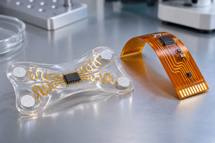
An elastic PCB is designed to accommodate tensile deformation, while a flexible PCB is primarily designed for bending and folding. Their materials, conductive structures, manufacturing processes, and reliability requirements are different.
| Feature | Elastic PCB | Flexible PCB |
|---|---|---|
| Mechanical Capability | Stretching, bending, twisting | Bending, folding |
| Common Substrates | TPU, PDMS, other elastomers | Polyimide (PI), PET |
| Conductive Structure | Stretchable composites, specially shaped metal interconnects | Primarily copper traces |
| Stretchability | Allowable strain depends on material and design | Not suitable for significant repeated stretching |
| Electrical Stability | Stretching may change resistance and impedance | Improper bending may cause copper fatigue and electrical failure |
| Component Mounting | Reinforced islands and strain-isolated regions | Solder pads and reinforced mounting areas |
| Reliability Testing | Stretch cycles, resistance drift, interface fatigue | Bend cycles, conductor fatigue, layer adhesion |
| Manufacturing | Specialized materials and interconnect processes | Established FPC manufacturing processes |
| Cost | Specialized processes and materials may increase cost | Conventional constructions generally offer more predictable costs |
| Typical Applications | Skin-mounted sensors, soft electronics | Wearable modules, medical device interconnections |
Actual manufacturing cost, reliability, and structural complexity depend on the circuit design, production quantity, and qualification requirements.
If the circuit must stretch with skin or another deformable surface, a conventional FPC is not a direct replacement. If the mechanical requirement is limited to bending or folding, a flexible PCB may provide a more practical option.
When Should You Choose a Flexible PCB Instead of an Elastic PCB?
A flexible PCB is generally a better choice when the circuit must bend, fold, or fit into a confined space without significant repeated stretching.
The following conditions favor conventional FPC technology:
-
Static Installation Bending: The circuit is bent into position during assembly and remains largely stationary afterward. A suitable FPC can accommodate the required geometry through appropriate thickness, bend radius, and trace layout.
-
Repeated Dynamic Bending: The circuit moves around a defined bending region. Copper type, stackup thickness, bending direction, and target cycle life must be evaluated to ensure adequate durability.
-
Compact Internal Interconnections: Smartwatches, hearing instruments, and portable medical devices often require flexible connections between electronic modules without exposing the circuit to substantial tensile strain.
-
Integrated Rigid and Flexible Sections: When rigid electronic components must be connected through flexible regions, a rigid-flex PCB can integrate stable mounting areas and flexible interconnections into one board construction.
For example, a wearable medical monitoring device may require stretchable electrodes at the skin interface, while its control circuit and display module only require flexible connections inside a compact enclosure. These sections can use different circuit technologies according to their mechanical requirements.
Before selecting a construction, identify whether the circuit experiences stretching or bending, its maximum displacement, minimum bend radius, expected movement cycles, and component locations.
If the application only requires controlled bending and reliable internal interconnections, a conventional flexible or rigid-flex PCB may reduce unnecessary material complexity and manufacturing cost.
Why Choose BestFPC for Your Flexible PCB Manufacturing?
BestFPC provides custom flexible and rigid-flex PCB manufacturing, free DFM check, and prototype-to-volume production support for electronic products requiring compact construction and reliable flexible interconnections.
For projects that do not require true circuit stretching, we help customers address manufacturing risks, complex stackups, rigid-to-flex transitions, and production requirements through the following services:
-
Identify Manufacturing Risks Before Production: Our free DFM check covers Gerber files, stackups, copper thickness, drilling requirements, and rigid-to-flex transitions. Identifying potential fabrication problems early helps reduce avoidable redesigns, repeated prototyping, and rework costs.
-
Manufacture Complex Rigid-Flex PCB Designs: We manufacture multilayer rigid-flex PCBs according to approved specifications and evaluate HDI, blind and buried vias, and controlled-impedance requirements against confirmed manufacturing capabilities. This supports compact electronic products with demanding interconnection requirements.
-
Reduce Connectors and Simplify Assembly: Integrating rigid mounting areas with flexible interconnections can replace selected board-to-board connectors and separate cables, helping save installation space and reduce connection-related failure risks.
-
Reduce Defects Through Quality Control: Material inspection, process control, automated optical inspection (AOI), and electrical testing help verify that manufactured boards meet approved requirements. ISO 9001 and ISO 13485 quality management documentation is also available for applicable supplier qualification reviews.
-
Support Prototypes and Volume Production: We support prototype evaluation, small-batch orders, and subsequent volume manufacturing based on the approved design, material requirements, and production schedule. This helps maintain consistent manufacturing specifications as projects move toward production.
From design-file evaluation to finished PCB delivery, BestFPC helps customers reduce manufacturing risks, control unnecessary rework costs, and obtain rigid-flex PCBs built to their approved specifications.
Frequently Asked Questions About Elastic PCB
Q1. Can an Elastic PCB Be Assembled Using Conventional SMT Reflow Processes?
A1: Conventional PCB reflow conditions cannot automatically be applied to elastic PCBs. TPU, PDMS, and certain stretchable conductive materials may not tolerate typical lead-free reflow temperatures. Circuits containing conventional electronic components may require reinforced mounting islands, compatible low-temperature bonding materials, or specialized assembly methods. The assembly process must be selected according to substrate temperature limits, component requirements, and the complete circuit construction.
Q2. How Can an Elastic PCB Be Connected to a Conventional Rigid PCB?
A2: Depending on the construction, connections can use conductive adhesives, specialized connectors, flexible transition structures, or locally reinforced contact regions. The main concern is preventing excessive tensile loading at the interface between the elastic circuit and the rigid PCB. Strain relief and mechanical isolation should be incorporated where necessary, with connection reliability verified through cyclic loading and electrical continuity testing.
Q3. Can Elastic PCBs Integrate Bluetooth or NFC Antennas?
A3: Yes, but antenna performance can change during stretching. Mechanical deformation may alter conductor length, spacing, resonant frequency, and impedance matching. For Bluetooth and NFC applications, antenna characteristics should be measured in both relaxed and specified stretched conditions. RF performance cannot be qualified solely through measurements taken before deformation, particularly where the antenna must operate while the device is moving.
Q4. Do Elastic PCBs Require Encapsulation on Both Sides?
A4: Not necessarily. Encapsulation depends on environmental exposure, stretching requirements, and the electrical interfaces involved. Double-sided encapsulation can provide protection against mechanical damage and moisture, but it may also increase overall stiffness and affect deformation behavior. Skin-contact electrodes and certain sensing regions may require exposed functional areas. Encapsulation thickness, adhesion, and mechanical compliance should be considered together during design.
Q5. How Much Current Can an Elastic PCB Carry?
A5: There is no universal current rating for elastic PCBs. Current capacity depends on conductor material, cross-sectional area, electrical resistance, thermal conditions, and changes caused by stretching. Copper traces, silver-based conductive composites, and liquid-metal channels have different electrical and thermal characteristics. Power-carrying interconnects should be evaluated for voltage drop, temperature rise, and conductivity stability under the specified mechanical conditions.
Q6. Are Elastic PCB Materials Suitable for Long-Term Skin Contact?
A6: Skin-contact suitability depends on the final product's material composition, contact duration, and intended medical use. Even when a medical-grade silicone is used, the complete circuit is not automatically biocompatible. Conductive materials, adhesives, encapsulation layers, and processing residues must also be considered. Medical applications may require biological safety evaluation under the applicable ISO 10993 requirements, based on the finished device and its intended contact conditions.
Q7. Are Gerber Files Sufficient for Custom Elastic PCB Manufacturing?
A7: Usually not. Gerber files describe conductor patterns but do not fully define the mechanical and material requirements of a stretchable circuit. Manufacturing specifications should also include substrate and conductor materials, layer construction, maximum working strain, stretching direction, target cycle life, allowable resistance changes, and assembly requirements. These details are necessary to evaluate manufacturing feasibility and establish meaningful reliability acceptance criteria.
Q8. Can Elastic PCBs Support Multilayer Circuits and Vias?
A8: Specialized multilayer stretchable structures are possible, but their interlayer connections are generally more challenging than those of conventional FPCs. Traditional plated vias located in high-strain areas may experience concentrated mechanical stress and eventual connection failure. Multilayer designs require careful consideration of via placement, interlayer adhesion, local reinforcement, and strain isolation, followed by electrical and mechanical validation.
Elastic PCB technology is suitable for electronic products that must withstand genuine tensile deformation, while flexible and rigid-flex PCBs are better suited to controlled bending, folding, and compact interconnections. Choosing the correct circuit structure helps avoid unsuitable materials, unnecessary manufacturing complexity, and potential reliability problems.
Are broken flex connections, damaged rigid-to-flex transitions, limited installation space, or repeated prototyping delays affecting your wearable or medical electronics project? If your product does not require true circuit stretching, BestFPC can provide custom flexible and rigid-flex PCB manufacturing, a free DFM check, manufacturing feasibility evaluation, and prototype-to-volume production support to help reduce fabrication risks and avoidable rework costs. Send your Gerber files, stackup, bending requirements, order quantity, and delivery location to sales@bestfpc.com for a custom manufacturing quotation.


.png)
.png)
.png)
.png)

.png)