


 2026-10-29

 BEST
Advanced rigid-flex PCB fabrication makes it possible to fit high-density circuits, multiple rigid sections, and flexible connections into compact electronic products. The challenge comes when fine-pitch routing, HDI vias, and complex layer structures must work together. A poorly planned stackup or rigid-to-flex transition can lead to manufacturing delays, assembly problems, or costly revisions.
BestFPC provides custom advanced rigid-flex PCB fabrication services, covering multilayer manufacturing, HDI processing, precision lamination, and PCB assembly. From complex stackup evaluation to finished-board production, we help customers overcome manufacturing challenges, reduce unnecessary design changes, and meet demanding project requirements.
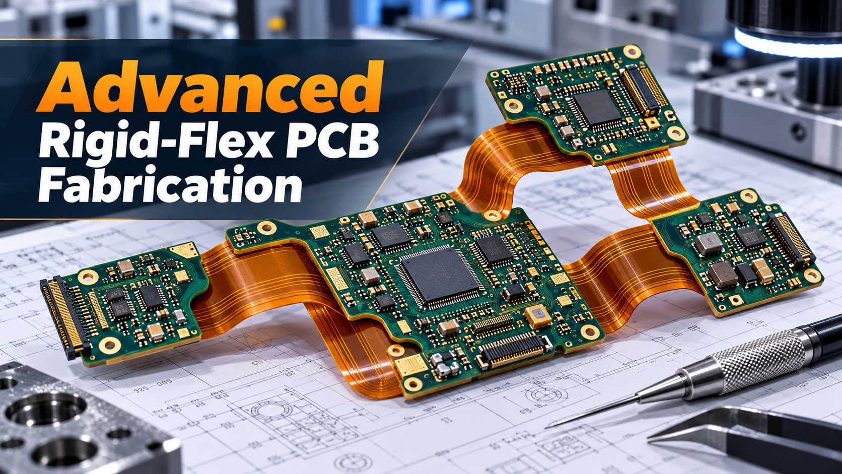
What Complex Designs Can Advanced Rigid-Flex PCB Fabrication Support?
Advanced rigid-flex PCB fabrication supports complex multilayer structures, high-density interconnections, and integrated flexible circuits that would otherwise require separate rigid boards, connectors, or cables.
BestFPC manufactures rigid-flex PCBs for a range of complex requirements:
-
Multilayer Rigid-Flex PCBs: Custom 4-layer, 6-layer, 8-layer, 12-layer, and other multilayer constructions for dense circuitry and compact assemblies.
-
HDI Rigid-Flex PCBs: Laser microvias, blind and buried vias, and fine-line routing for BGA, WLCSP, and other high-density components.
-
Multi-Section Rigid-Flex PCBs: Multiple rigid areas connected by flexible circuits, allowing components to fit into different positions within an enclosure.
-
Controlled-Impedance Rigid-Flex PCBs: Multilayer constructions with defined dielectric thicknesses and transmission-line geometries for high-speed signal applications.
-
Complex Bending Structures: Thin flexible connections, folded configurations, and specialized rigid-to-flex transitions for restricted installation spaces.
A complex rigid-flex PCB cannot be evaluated by layer count alone. Copper thickness, via arrangement, flex geometry, and material construction all influence manufacturing feasibility.
BestFPC reviews these requirements together before confirming the manufacturing approach, particularly for designs combining HDI technology with multiple flexible sections.
Which Stackup and Material Options Are Available for Complex Rigid-Flex PCBs?
BestFPC supports custom multilayer rigid-flex PCB stackups, including 4-layer, 6-layer, 8-layer, and 12-layer constructions. Different copper layer counts can be used in the rigid and flexible sections, providing additional routing space where components are mounted while keeping the flexible connections thinner.
Common rigid-flex PCB stackup configurations include:
-
4-Layer Rigid-Flex PCB (2 Rigid-Only + 2 Flex Layers): Four copper layers are available in the rigid sections, while two inner layers extend through the flexible connection. This construction suits compact sensor modules, portable electronics, and products requiring relatively simple folded interconnections.
-
6-Layer Rigid-Flex PCB (4 Rigid-Only + 2 Flex Layers): Six conductive layers are present in the rigid sections, with two inner layers continuing through the flexible area. The additional rigid-only layers provide more space for signal routing, power distribution, and component connections without increasing the flexible section to six copper layers.
-
8-Layer Rigid-Flex PCB (2 or 4 Flex Layers): An eight-layer structure can use two continuous flexible layers for a thinner interconnection or four flexible layers when additional routing is required. It is suitable for complex electronic assemblies with multiple rigid sections and higher interconnection density.
-
10-Layer and 12-Layer Rigid-Flex PCBs: Higher-layer-count constructions provide more routing and reference-plane options for dense electronic designs. Blind and buried vias, HDI microvias, and sequential buildup structures can be incorporated where the complete stackup supports the required interconnections.
-
Air-Gap and Bookbinder Rigid-Flex Stackups: These specialized structures use separated flexible sub-stacks to accommodate demanding folding requirements. Bookbinder constructions use different flex lengths to account for the bending paths of inner and outer layers, reducing unwanted stretching or buckling during installation.
Material Options for Complex Rigid-Flex Stackups
-
Rigid Substrates: FR-4 and high-Tg laminates provide mechanical support, dimensional stability, and suitable mounting areas for electronic components.
-
Flexible Substrates: Polyimide (PI) laminates, including adhesiveless constructions, provide flexibility and thermal resistance. Thinner PI constructions can help reduce the finished flex thickness.
-
Copper Foils: Rolled annealed (RA) and electrodeposited (ED) copper are selected according to electrical requirements, conductor thickness, and expected bending conditions.
-
Bonding Materials: Compatible prepreg and controlled-flow bonding systems maintain adhesion while limiting unwanted resin flow around exposed flexible sections.
-
Protective Materials: Polyimide coverlay protects flexible circuitry, while compatible solder mask and surface finishes are applied according to the rigid and flexible region requirements.
The correct stackup depends on the number of signals crossing the flex region, finished thickness, bend radius, and required layer connections. Not every layer arrangement or special construction is suitable for every project.
BestFPC reviews the proposed layer distribution, materials, HDI structures, and mechanical requirements to determine a manufacturable rigid-flex PCB construction.
How Does the Advanced Rigid-Flex PCB Fabrication Process Work?
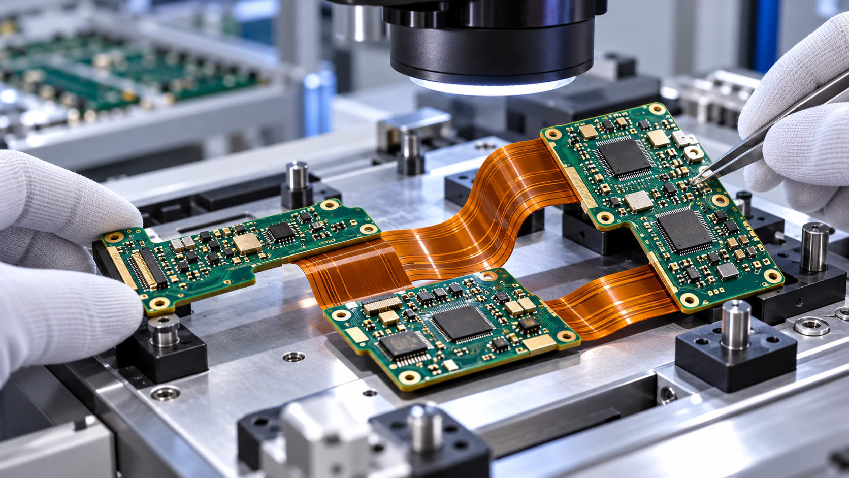
Advanced rigid-flex PCB fabrication combines flexible-circuit processing, multilayer lamination, precision drilling, copper plating, and final profiling. The manufacturing process must protect flexible regions while maintaining accurate electrical connections throughout the multilayer structure.
The main manufacturing stages include:
-
Material Preparation and Inner-Layer Fabrication: FR-4, PI laminates, copper foils, and bonding materials are prepared according to the approved stackup. Inner-layer circuits are formed through imaging and etching, followed by inspection of critical conductor features.
-
Flexible-Layer Processing: Flexible circuits are fabricated and protected with polyimide coverlay where required. Coverlay openings and rigid-to-flex boundaries are formed according to the approved construction.
-
Multilayer Alignment and Lamination: Rigid and flexible layers are aligned and laminated under controlled conditions. Bonding materials and lamination parameters are selected to maintain adhesion without excessive resin flow into the flexible regions.
-
Drilling and HDI Via Formation: Mechanical and laser drilling create the required holes and microvias. Blind and buried via structures may require additional drilling, plating, and sequential lamination operations.
-
Outer-Layer Fabrication and Surface Finishing: External circuits are formed through copper plating, imaging, and etching. Solder mask is applied where specified, followed by the selected surface finish, such as ENIG or ENEPIG.
-
Final Profiling and Inspection: Rigid material is removed from designated flex openings, and the final outline is formed. Electrical testing, dimensional inspection, and agreed acceptance checks are completed before shipment.
For HDI rigid-flex PCB fabrication, the drilling and lamination sequence depends on the connections required between layers. Stacked microvias and complex buried vias may require several buildup cycles, making accurate registration especially important.
What Are the Common Challenges in Complex Rigid-Flex PCB Fabrication?
Complex rigid-flex PCB fabrication involves several challenges that can affect electrical connections, bending performance, and dimensional accuracy. BestFPC addresses these problems by adapting the materials and manufacturing processes to the approved board construction.
1. Multilayer Registration and Alignment
Challenge: Different expansion characteristics of FR-4 and polyimide can cause layer misalignment during lamination. In HDI designs, registration errors may affect microvia connections and fine-pitch routing.
BestFPC Solution: We use dimensional compensation, controlled layer registration, and precision lamination alignment. Inner-layer inspection helps identify registration problems before additional layers are processed.
2. Resin Flow and Delamination
Challenge: Excessive resin flow near rigid-to-flex transitions can restrict bending, while inadequate bonding may cause separation between rigid and flexible materials during thermal or mechanical stress.
BestFPC Solution: We select compatible bonding materials and control lamination temperature, pressure, and material placement. Defined bonding boundaries help maintain adhesion without restricting the intended flexible regions.
3. HDI Microvia and Buried Via Reliability
Challenge: Complex HDI structures require accurate drilling, copper deposition, and multilayer registration. Poor metallization or unsuitable via arrangements can weaken electrical connections, particularly during thermal cycling.
BestFPC Solution: We coordinate laser drilling, internal via processing, copper plating, and sequential lamination according to the required interconnection structure. Critical via constructions can also be evaluated through microsection inspection and additional reliability checks.
4. Copper Cracking at Rigid-to-Flex Transitions
Challenge: Mechanical stress concentrates near rigid-to-flex boundaries. Thick copper, unsuitable conductor placement, or an insufficient bend radius can increase the risk of cracking.
BestFPC Solution: We review copper construction, flex thickness, coverlay termination, and transition geometry. Suitable copper materials and controlled bending structures help reduce localized stress, especially when the flexible connection is exposed to repeated movement.
5. Board Warpage and Thickness Variation
Challenge: Uneven copper distribution, material buildup, and multiple lamination cycles can cause warpage or inconsistent thickness. These problems may interfere with connector alignment, mounting, and SMT assembly.
BestFPC Solution: We control copper balance, lamination conditions, and panel handling. Finished rigid and flexible thicknesses are checked against the approved specifications to maintain dimensional compatibility.
6. Controlled-Impedance Variation
Challenge: Changes in dielectric materials, trace geometry, and reference planes between rigid and flexible sections can affect signal impedance.
BestFPC Solution: We review dielectric thickness, conductor dimensions, and reference-plane arrangements against the required impedance targets. Impedance verification can be included for designs with specified signal-integrity requirements.
Each manufacturing solution depends on the actual stackup and operating conditions. A rigid-flex PCB intended for a single installation fold may require a different construction from one exposed to continuous bending or vibration.
What Affects Advanced Rigid-Flex PCB Fabrication Cost and Lead Time?
The cost and lead time of advanced rigid-flex PCB fabrication depend mainly on layer structure, HDI complexity, material selection, and production quantity. Boards with the same number of layers may require different manufacturing operations and therefore have different quotations.
| Fabrication Requirement | Cost Impact | Lead Time Impact |
|---|---|---|
| Conventional multilayer rigid-flex PCB | Layer count, material usage, and panel utilization | Multilayer processing and profiling |
| HDI rigid-flex PCB | Laser drilling, fine-line fabrication, and additional plating | Additional drilling and inspection |
| Blind and buried vias | Internal via processing and extra lamination operations | More complex fabrication sequence |
| Stacked microvias | Via filling, registration, and sequential buildup | Multiple buildup and verification stages |
| Specialized flexible materials | Material selection, bonding requirements, and availability | Possible additional procurement time |
| Complex rigid-flex outlines | Reduced panel utilization and additional profiling | More demanding handling and profiling |
| PCB fabrication with assembly | Component sourcing, SMT processing, fixtures, and inspection | Additional procurement and assembly stages |
A four-layer rigid-flex PCB using conventional vias may require fewer manufacturing operations than a six-layer HDI rigid-flex PCB containing blind vias and multiple buildup cycles.
BestFPC evaluates the complete fabrication requirements before quoting. Material availability, the approved stackup, order quantity, and assembly needs are considered when establishing the production schedule.
How Do You Choose a Reliable Advanced Rigid-Flex PCB Fabrication Supplier?
A reliable advanced rigid-flex PCB fabrication supplier should have proven experience with complex stackups, HDI interconnections, and precision multilayer manufacturing. Its capabilities must match the complete PCB construction, not just individual specifications.
When comparing rigid-flex PCB manufacturers, focus on these five factors:
-
Manufacturing Capability: Check supported layer counts, minimum line width and spacing, microvia dimensions, copper thickness, and rigid-flex thickness tolerances. A manufacturer capable of producing 0.060 mm microvias may not support that dimension in every multilayer rigid-flex stackup. Confirm the complete combination before ordering.
-
Complex Rigid-Flex Experience: Look for experience with HDI, blind and buried vias, multiple rigid sections, and controlled-impedance structures. Similar manufacturing projects provide stronger evidence than general claims about advanced PCB technology.
-
Quality Certifications and Reliability: Confirm applicable ISO certifications, IPC requirements, material traceability, and electrical inspection capabilities. For medical, automotive, or aerospace projects, verify that the quality management system covers the relevant manufacturing activities.
-
Engineering and Technical Support: A capable supplier should review Gerber files, stackup construction, flex thickness, via arrangements, and bending requirements before production. Clear explanations of manufacturing limitations help customers avoid unexpected design revisions.
-
Cost, Lead Time, and Assembly Services: Compare complete quotations rather than bare-board prices alone. Confirm material availability, fabrication schedules, component sourcing, assembly capabilities, and delivery commitments to avoid additional costs or delays.
The right supplier should provide a clear assessment of manufacturing feasibility, realistic delivery conditions, and the documentation needed to qualify the finished PCB.
Why Choose BestFPC for Advanced Rigid-Flex PCB Fabrication Services?
BestFPC provides advanced rigid-flex PCB fabrication, engineering support, and one-stop PCB assembly, helping customers manufacture complex designs, reduce supplier coordination, and meet demanding project requirements.
-
Advanced Multilayer and HDI Capabilities: Support custom rigid-flex PCBs, including 12-layer constructions, blind and buried vias, and fine-line circuitry. Advanced HDI capabilities include 0.060/0.060 mm inner-layer line/space and 0.060 mm laser microvias for applicable constructions, providing more routing options for high-density designs.
-
Free DFM Review and Engineering Support: Identify potential manufacturing problems before production, including stackup conflicts, via arrangements, and rigid-to-flex transitions. This helps customers avoid unnecessary design revisions and prototype delays.
-
One-Stop PCB Manufacturing and Assembly: Provide PCB fabrication, component sourcing, SMT, THT, and inspection services. Customers can coordinate fabrication and assembly through one supplier, reducing communication work and unnecessary production handoffs.
-
Certified Quality Management: BestFPC provides quality-management documentation for ISO 9001, ISO 13485, IATF 16949, and AS9100D, subject to applicable certification and facility scope. Supporting documents can assist with supplier qualification and industry-specific purchasing requirements.
-
Flexible Prototype and Production Support: Accommodate prototype quantities, small batches, and repeat production orders while maintaining approved manufacturing specifications across production stages.
-
Delivery and Engineering Communication: Coordinate material availability, manufacturing schedules, and shipping requirements. Customers receive project-specific delivery arrangements and technical updates when manufacturing issues require clarification.
With specialized rigid-flex fabrication, free engineering review, and integrated PCB assembly, BestFPC helps customers manage complex manufacturing projects with fewer supplier handoffs.
How Does BestFPC Handle Complex Rigid-Flex PCB Fabrication Projects?
BestFPC has completed a seven-layer HDI rigid-flex PCB project incorporating blind and buried vias, demonstrating manufacturing experience with complex multilayer interconnections and controlled-impedance requirements.
Project Background
The project involved a seven-layer rigid-flex PCB with HDI interconnections. Blind and buried vias were required to connect selected copper layers within the multilayer construction.
Technical Requirements and Challenges
The board specifications included 1.40 mm finished thickness, 0.10 mm minimum hole size, 1 oz outer-layer copper, 0.5 oz inner-layer copper, and ENIG surface finishing.
The design also specified 50 Ω single-ended and 100 Ω differential impedance targets. The main challenge was integrating the different via structures while maintaining the required copper construction, dielectric arrangement, and finished dimensions.
BestFPC Manufacturing Solution
BestFPC coordinated internal buried via processing, copper plating, and multilayer lamination with the subsequent blind via operations.
The fabrication approach also accounted for conductor geometry and dielectric construction to accommodate the specified impedance targets.
Manufacturing Result
BestFPC completed the seven-layer HDI rigid-flex PCB with blind and buried vias, a 1.40 mm finished construction, and ENIG surface finishing.
The project demonstrates BestFPC's experience manufacturing complex multilayer rigid-flex structures that combine different interconnection technologies within one board.
FAQs About Advanced Rigid-Flex PCB Fabrication
Q1: Can electronic components be mounted directly on flexible PCB sections?
A1: Yes, when suitable mechanical support and strain relief are provided. Components are generally mounted in rigid or reinforced areas to reduce stress on solder joints.
Q2: Can rigid-flex PCBs be folded after SMT assembly?
A2: Yes, if the board is designed for the intended installation bend. Bend radius, component positions, and mechanical strain must be considered.
Q3: What Is the Difference Between Static-Flex and Dynamic-Flex Rigid-Flex PCBs?
A3: Static-flex boards are generally bent during installation and remain in position. Dynamic-flex boards are designed for repeated movement and require suitable copper construction, flex thickness, and bending geometry.
Q4: Can vias be placed in rigid-flex PCB bending areas?
A4: Vias should generally be kept outside active bending regions because they create local stress concentrations. Any exception requires specific mechanical and manufacturing review.
Q5: Can rigid-flex PCBs be supplied in panels for automated SMT assembly?
A5: Yes. Panelization and assembly fixtures can be arranged around rigid sections, flexible connections, and component locations.
Q6: Can flexible sections use ZIF connector contacts?
A6: Yes. Flexible tails can be manufactured for compatible ZIF connectors when contact pitch, finished thickness, surface finish, and reinforcement requirements are correctly specified.
Q7: Can stiffeners be added to flexible sections?
A7: Yes. FR-4 or polyimide stiffeners can reinforce connector areas and component mounting locations without adding conductive rigid-board layers.
Q8: How should rigid-flex PCBs be stored before assembly?
A8: Keep boards protected from moisture, contamination, and mechanical deformation. Storage and pre-assembly handling requirements depend on the materials, packaging, and approved assembly process.
How Can You Get a Custom Advanced Rigid-Flex PCB Fabrication Quote?
BestFPC provides advanced rigid-flex PCB fabrication, free preliminary DFM review, and one-stop PCB assembly services for complex multilayer and HDI projects.
Send your Gerber files or ODB++ data, stackup, quantity, required delivery date, and delivery location, along with any special material, impedance, bending, or assembly requirements.
Contact BestFPC at sales@bestfpc.com for a free DFM review and custom advanced rigid-flex PCB fabrication quotation.


.png)
.png)
.png)
.png)

.png)