


 2026-10-28

 BEST
Looking for a reliable 8-layer rigid-flex PCB manufacturer? BestFPC provides custom 8-layer rigid-flex PCB fabrication, HDI processing, precision multilayer lamination, and free DFM reviews. We support complex stackups, blind and buried vias, controlled impedance, and rigid-to-flex transitions for prototypes and volume production.
An 8-layer rigid-flex PCB combines high-density circuitry with flexible interconnections, reducing separate connectors and installation space. Reliable manufacturing requires accurate layer registration, suitable materials, controlled via processing, and proper bending geometry.

What Is an 8-Layer Rigid-Flex PCB?
An 8-layer rigid-flex PCB integrates rigid circuit sections and flexible interconnections into one multilayer board. The rigid regions contain up to eight conductive copper layers, while the flexible regions typically use fewer layers to maintain flexibility.
Rigid sections accommodate high-density components, signal routing, power distribution, and ground planes. Flexible sections connect these areas without separate cables or connectors.
This construction is particularly useful for electronic assemblies requiring high routing density, compact packaging, and reliable electrical connections.
When Do You Need an 8-Layer Rigid-Flex PCB?
An 8-layer rigid-flex PCB is suitable when a lower-layer-count design cannot accommodate the required signal routing, reference planes, power distribution, and mechanical layout.
Typical requirements include:
-
High-Density BGA Routing: Fine-pitch components and complex interconnections requiring additional signal layers or HDI vias.
-
High-Speed Signals: Controlled-impedance routing with appropriate ground references and signal separation.
-
Multiple Power Rails: Additional copper layers for power distribution and ground connections.
-
Compact 3D Assemblies: Multiple rigid circuit sections connected through flexible regions within limited installation space.
-
Connector Reduction: Integrated flexible connections that eliminate selected board-to-board connectors and their associated failure points.
For example, a compact medical controller containing a processor, power-management circuitry, and multiple sensors may require eight copper layers in its rigid sections but only two in the flexible interconnection.
An eight-layer structure is most useful when the additional routing capacity solves a specific electrical or mechanical constraint.
How Is an 8-Layer Rigid-Flex PCB Stackup Designed?
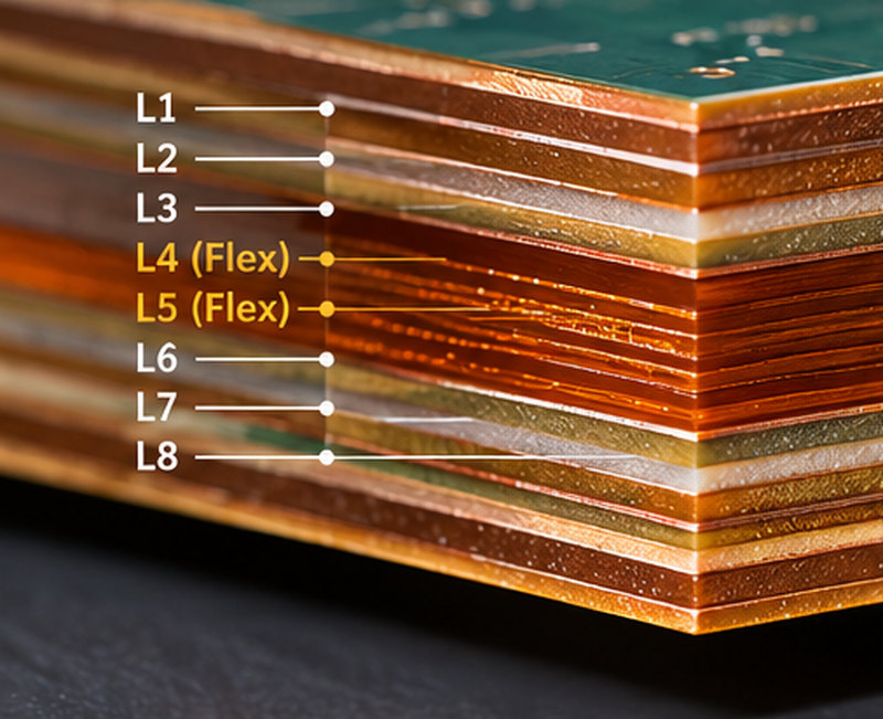
An 8-layer rigid-flex PCB stackup combines eight copper layers in the rigid sections with a thinner flexible interconnection. A common configuration uses eight rigid-region layers and two continuous flexible layers.
| Copper Layer | Primary Function | Rigid Section | Flexible Section |
|---|---|---|---|
| L1 | Component pads and signal routing | Yes | No |
| L2 | Ground reference plane | Yes | No |
| L3 | Internal signal routing | Yes | No |
| L4 | Signal interconnection | Yes | Yes |
| L5 | Signal return/reference conductors | Yes | Yes |
| L6 | Power distribution | Yes | No |
| L7 | Ground reference plane | Yes | No |
| L8 | Component pads and signal routing | Yes | No |
The L4–L5 flexible core provides continuous electrical connections between the rigid sections, while the remaining copper layers provide additional routing capacity within the rigid regions.
A four-layer flexible section may be selected when more connections must cross the bend region, but its increased thickness generally requires a larger bend radius.
For controlled-impedance designs, the stackup must also account for dielectric thickness, copper geometry, reference conductors, and the electrical properties of the selected materials.
Which Materials Are Suitable for 8-Layer Rigid-Flex PCBs?
FR-4, polyimide (PI), copper foil, coverlay, and low-flow bonding materials are commonly used in 8-layer rigid-flex PCB manufacturing.
| Material | Application | Key Selection Requirements |
|---|---|---|
| FR-4 Laminate | Rigid sections | Tg, thermal expansion, dielectric properties, thickness |
| Adhesiveless PI | Flexible circuit core | Flexibility, dimensional stability, thickness |
| RA Copper | Flex conductors requiring improved fatigue performance | Copper thickness, ductility, bend requirements |
| ED Copper | Suitable rigid or flexible circuitry | Copper thickness, surface profile, mechanical requirements |
| PI Coverlay | Flexible conductor protection | Opening accuracy, thickness, adhesive compatibility |
| Low-Flow / No-Flow Prepreg | Rigid-flex lamination | Resin-flow control, bonding strength, dielectric thickness |
Adhesiveless PI helps reduce flexible-region thickness, while RA copper is often preferred for circuits exposed to demanding bending conditions.
Material selection must also account for current capacity, soldering temperature, and thermal expansion. Higher copper thickness increases conductor cross-section but also makes the flexible section stiffer.
How Should Microvias, Blind Vias, and Buried Vias Be Used in 8-Layer Rigid-Flex PCBs?
Microvias, blind vias, and buried vias support high-density routing by connecting selected copper layers without requiring every interconnection to pass through the full board thickness.
| Via Type | Typical Application | Manufacturing Process |
|---|---|---|
| Blind Microvia | L1–L2 BGA escape routing | Laser drilling and copper plating |
| Buried Via | Internal rigid-section layer connections | Internal drilling and plating before subsequent lamination |
| Plated Through-Hole | Connections through all eight rigid-region layers | Mechanical drilling and copper plating |
| Stacked Microvia | High-density vertical layer connections | Sequential buildup with suitable via filling and plating |
Fine-pitch BGAs may use L1–L2 blind microvias to access inner routing layers. Buried vias can preserve outer-layer routing space, provided the internal connections are compatible with the lamination sequence.
Stacked microvias require additional attention to copper filling, alignment, and thermal reliability. The selected HDI structure must be manufacturable within the actual eight-layer stackup.
Plated vias should normally remain outside active bending regions, where repeated mechanical strain can damage the copper interconnections.
What Are the Key Design Rules for 8-Layer Rigid-Flex PCBs?
Reliable 8-layer rigid-flex PCB design requires accurate control of bending geometry, copper routing, and rigid-to-flex transition areas.
-
Define the Bend Radius: Determine the required radius from flexible-region thickness, bend angle, and operating conditions. Static installation bends and repeated dynamic bending require different constructions.
-
Keep Vias Outside Bend Areas: Place plated holes and component pads in rigid or appropriately supported regions whenever possible.
-
Control Trace Routing: Route conductors approximately perpendicular to the bend axis. Avoid sharp corners and abrupt width changes, and stagger traces on adjacent layers where suitable.
-
Protect Rigid-to-Flex Transitions: Avoid sharp internal corners, poorly positioned coverlay terminations, and unsupported conductors near rigid laminate edges.
-
Limit Copper Stiffness: Reduce unnecessary copper in bending regions. Copper patterns must still meet current-carrying, grounding, and signal-integrity requirements.
-
Specify Mechanical Dimensions: Include rigid and flex thicknesses, bend locations, angles, minimum radii, and expected bending cycles in the fabrication drawing.
IPC-2223 provides relevant design guidance. Final bend requirements must be evaluated against the complete flex construction rather than the total rigid-section layer count.
What Manufacturing Capabilities Are Required for 8-Layer Rigid-Flex PCBs?
An experienced 8-layer rigid-flex PCB manufacturer needs precise multilayer registration, fine-line processing, reliable copper plating, controlled lamination, and accurate rigid-to-flex profiling.
BestFPC supports the following manufacturing specifications.
| Manufacturing Parameter | BestFPC Capability |
|---|---|
| Rigid-Flex PCB Layers | 2–20 layers |
| Finished Board Thickness | 0.30–3.00 mm |
| Inner-Layer Line Width / Spacing | 3/3 mil (0.076/0.076 mm) |
| Rigid Outer-Layer Line Width / Spacing | 3.5/3.5 mil (0.089/0.089 mm) |
| Flexible Outer-Layer Line Width / Spacing | 5/4.5 mil (0.127/0.114 mm) |
| Mechanical Drill Diameter | 0.15 mm for applicable thicknesses ≤1.60 mm |
| Additional Mechanical Drill Option | 0.20 mm for applicable thicknesses ≤2.50 mm |
| Adhesiveless PI Base Copper Options | 0.33, 0.5, 1, and 2 oz |
| HDI Processing | Blind and buried vias |
| Surface Finish | ENIG, plated gold, OSP, tin plating |
| Controlled Impedance | Available with an approved stackup and tolerance |
The line-width and spacing limits apply to specified 18 μm finished-copper conditions before manufacturing compensation. Mechanical drill values are drill-tool diameters, not finished plated-hole sizes.
The achievable combination of layer count, copper thickness, holes, and minimum features depends on the complete construction.
BestFPC's free DFM review checks these requirements together before fabrication, helping identify stackup conflicts, drill limitations, and rigid-to-flex transition risks.
How Is an 8-Layer Rigid-Flex PCB Manufactured?
8-layer rigid-flex PCB manufacturing involves flexible circuit processing, multilayer lamination, precision drilling, copper plating, and selective removal of rigid materials.
-
Material Preparation: Prepare the approved FR-4 laminates, PI cores, copper foils, and bonding materials according to the stackup.
-
Flexible Inner-Layer Fabrication: Image and etch the flexible copper circuits, inspect the traces, and process coverlay at the appropriate manufacturing stage.
-
Buried-Via Processing: Drill and plate the required internal subassemblies before subsequent lamination encloses the connections.
-
Multilayer Lamination: Align the rigid and flexible materials, controlling pressure, temperature, resin flow, and layer registration.
-
Drilling and HDI Processing: Perform mechanical drilling, laser microvia processing, copper plating, and additional buildup operations where required.
-
Outer-Layer Processing: Form the outer copper patterns, apply protective layers, and complete the specified surface finish.
-
Profiling and Flex-Region Release: Form the board outline and remove designated rigid materials to expose the flexible sections.
-
Inspection and Electrical Testing: Perform applicable AOI, dimensional inspection, continuity and isolation testing, and additional verification required by the approved specifications.
For complex eight-layer constructions, multilayer registration, plated interconnection integrity, and rigid-to-flex transition quality have a direct influence on manufacturing reliability.

What Affects 8-Layer Rigid-Flex PCB Cost and Lead Time?
8-layer rigid-flex PCB cost and lead time depend on manufacturing complexity, material requirements, HDI structures, production quantity, and inspection requirements.
| Manufacturing Factor | Cost Impact | Lead Time Impact |
|---|---|---|
| Complex Stackup | Additional lamination and processing | More production stages |
| Blind and Buried Vias | Additional drilling, plating, and buildup operations | Longer processing sequence |
| Fine-Line Circuitry | Higher precision and yield requirements | Additional process control |
| Special Materials | Material and procurement costs | Possible sourcing delays |
| Board Geometry | Panel utilization and profiling complexity | Additional handling and profiling |
| Production Quantity | Setup and tooling cost distribution | Depends on batch size and capacity |
| Special Testing | Additional inspection and qualification | Additional verification time |
For prototype production, finalized stackup data and complete fabrication files help reduce manufacturing revisions. For volume production, approved materials and consistent acceptance requirements support repeatability.
BestFPC confirms prototype and production lead times based on the actual stackup, quantity, materials, and processing requirements.
Why Choose BestFPC as Your 8-Layer Rigid-Flex PCB Manufacturer?
BestFPC provides custom 8-layer rigid-flex PCB manufacturing, engineering support, free DFM review, and assembly services for complex multilayer projects.
-
Advanced Manufacturing: Multilayer rigid-flex fabrication, HDI processing, fine-line circuitry, blind and buried vias, and precision lamination support demanding PCB constructions.
-
Free DFM Review: Our engineers check stackups, copper thicknesses, via structures, bending regions, coverlay openings, and critical tolerances before production.
-
Quality Certifications: BestFPC provides quality management documentation covering ISO 9001, ISO 13485, IATF 16949, and AS9100D. Current certificates and applicable manufacturing scopes can be requested for supplier qualification.
-
Strict Quality Control: Material inspection, AOI, electrical testing, and agreed additional verification help ensure the finished boards meet their manufacturing specifications.
-
One-Stop PCB Services: Bare-board fabrication, component sourcing, SMT assembly, and testing reduce coordination between different manufacturing suppliers.
-
Fast Prototype and Production Support: Prototype, small-batch, and repeat orders are supported with manufacturing planning based on confirmed project requirements.
Send your Gerber or ODB++ files, stackup, quantity, target delivery date, and delivery location to sales@bestfpc.com. BestFPC will review your manufacturing requirements and provide DFM feedback and a quotation for your 8-layer rigid-flex PCB project.
FAQs About 8-Layer Rigid-Flex PCB Manufacturing
Q1: What Is the Minimum Order Quantity for an 8-Layer Rigid-Flex PCB?
A1: BestFPC supports prototype and small-batch orders. Minimum quantities and order conditions are confirmed according to the construction and manufacturing requirements.
Q2: Can BGA Components Be Mounted on Both Sides of the Rigid Sections?
A2: Yes. Double-sided BGA assembly is possible when board thickness, component clearance, pad design, and reflow requirements are suitable.
Q3: Can 8-Layer Rigid-Flex PCBs Be Supplied in Panels for SMT Assembly?
A3: Yes. Panelization depends on board geometry, tooling, rigid-section support, and assembly handling requirements.
Q4: Is ENIG Suitable for Fine-Pitch BGA Assembly?
A4: Yes. ENIG provides a relatively planar, solderable finish suitable for many fine-pitch BGA applications.
Q5: Can Different Rigid Sections Have Different Finished Thicknesses?
A5: Yes, selected rigid-flex constructions can support different regional thicknesses. The stackup and fabrication method require engineering review.
Q6: Can BestFPC Provide Impedance Test Reports?
A6: Impedance testing and supporting reports can be arranged according to the approved stackup and agreed acceptance requirements.
Q7: Can I Order Bare 8-Layer Rigid-Flex PCBs Without Assembly?
A7: Yes. BestFPC provides bare-board fabrication. Component sourcing, SMT assembly, and additional testing can be included when required.
Q8: What Information Should I Include in My RFQ?
A8: Provide Gerber or ODB++ files, drill data, stackup, fabrication drawings, bend requirements, order quantity, target delivery date, and delivery location.


.png)
.png)
.png)
.png)

.png)