


 2026-11-13

 BEST
A strain gauge PCB can connect a sensing element to its readout electronics or carry the circuitry used to process its signal. For OEM projects, the manufacturing specification should distinguish the sensing grid, the interconnect, and the assembled readout board. Each has different material, mechanical, and acceptance requirements.
At BestFPC, quality is the real test. That’s why we support your project with DFM reviews, BOM optimization recommendations, and prototype builds to help resolve manufacturing issues before volume production. We manufacture custom flexible and rigid-flex circuits for sensor interconnections and provide PCB assembly to approved customer designs. Send your drawings to sales@bestfpc.com to discuss your manufacturing requirements.
What Strain Gauge PCB Types Can BestFPC Manufacture?
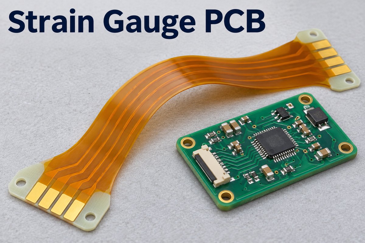
We supply copper-based flexible circuits and rigid-flex boards for strain measurement assemblies. The appropriate board type depends on where the sensing element sits, how the signal reaches the electronics, and whether components need a rigid mounting area.
| Board Type | Typical Application | Structural Benefit |
|---|---|---|
| Single-sided FPC | Short sensor-to-board connections | Simple routing in restricted spaces |
| Double-sided FPC | Multiple sensor leads and return paths | Routing on both copper layers |
| Multilayer FPC | Denser sensor interconnections | Additional routing and plane options |
| Rigid-flex PCB | Integrated sensor readout modules | Rigid component areas with flexible links |
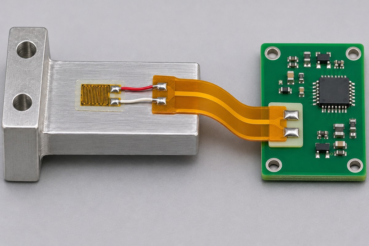
A flex circuit can connect an externally mounted strain gauge to a separate amplifier board. A rigid-flex construction can instead connect the sensor interface to a rigid section carrying the readout electronics. Bare-board supply and assembled-board supply are defined separately in the order.
Specialized resistive grids require their own material and process assessment. Specifying a copper FPC does not establish that its traces are suitable as the strain-sensitive element.
PCB Strain Gauge Interconnect Manufacturing Capabilities
Our PCB strain gauge interconnect manufacturing uses PI substrates, copper conductors, local reinforcement, and specified surface finishes. We review the stackup and terminal geometry together so that the finished circuit fits the intended assembly.
| Manufacturing Item | Available Options | Selection Requirement |
|---|---|---|
| FPC layer count | 1–4 layers | Routing and installation needs |
| Rigid-flex layer count | 2–20 layers | Approved rigid-flex stackup |
| Adhesive PI core | 0.5, 1, or 2 mil PI | Copper and adhesive combination |
| Adhesiveless PI core | 0.5, 1, 2, or 3 mil PI | Stackup and flex-zone requirements |
| Adhesive-core copper | 0.33, 0.5, or 1 oz | Trace geometry and resistance budget |
| Adhesiveless-core copper | 0.33, 0.5, 1, or 2 oz | Routing and mechanical requirements |
| PI stiffener material | 3, 5, 7, or 9 mil | Required finished terminal thickness |
| Surface finish | ENIG, gold plating, OSP, tin plating | Soldering or contact requirements |
These are individual manufacturing options, not a guarantee that every combination is suitable for one design. PI thickness refers to the core film, while stiffener thickness excludes the rest of the terminal stack. Connector fit must be checked against the total finished thickness, including copper, adhesive, coverlay, and reinforcement where applicable.
For sensor leads, copper thickness and trace geometry should follow the circuit’s resistance requirements. Increasing copper thickness may help one electrical requirement while changing the mechanical behavior of the flex section; the complete stackup needs review.
Strain Gauge on PCB: DFM Review Before Manufacturing
For a project involving a strain gauge on PCB, our DFM review focuses on whether the board can be manufactured and integrated as drawn. We identify fabrication and assembly issues before tooling and production release.
- Gauge installation area: Mark the intended bonding or mounting region and its surface requirements. Unspecified solder mask, coverlay, or raised features can interfere with the customer’s installation method.
- Lead termination: Define solder pads, connector contacts, or through-hole pins with their dimensions and access requirements. For a strain gauge connection using a through-hole pin on the PCB, specify the finished hole and pin dimensions together.
- Flex transition: Show the installed bend location and the boundary of each stiffener. Keep the intended bending section distinct from component and termination areas.
- Trace and pad geometry: Review line width, spacing, copper thickness, and coverlay openings as a combination. Narrow features that are manufacturable on one stackup may require changes on another.
- Assembly access: Provide component placement and mechanical constraints so that connectors, soldering tools, and inspection equipment can reach the necessary areas.
The resulting DFM report gives your engineer specific items to approve or revise. Strain gauge PCB design ownership, sensor selection, and system calibration remain separate from this manufacturing review.
Strain Gauge PCB Assembly for Sensor Readout Modules
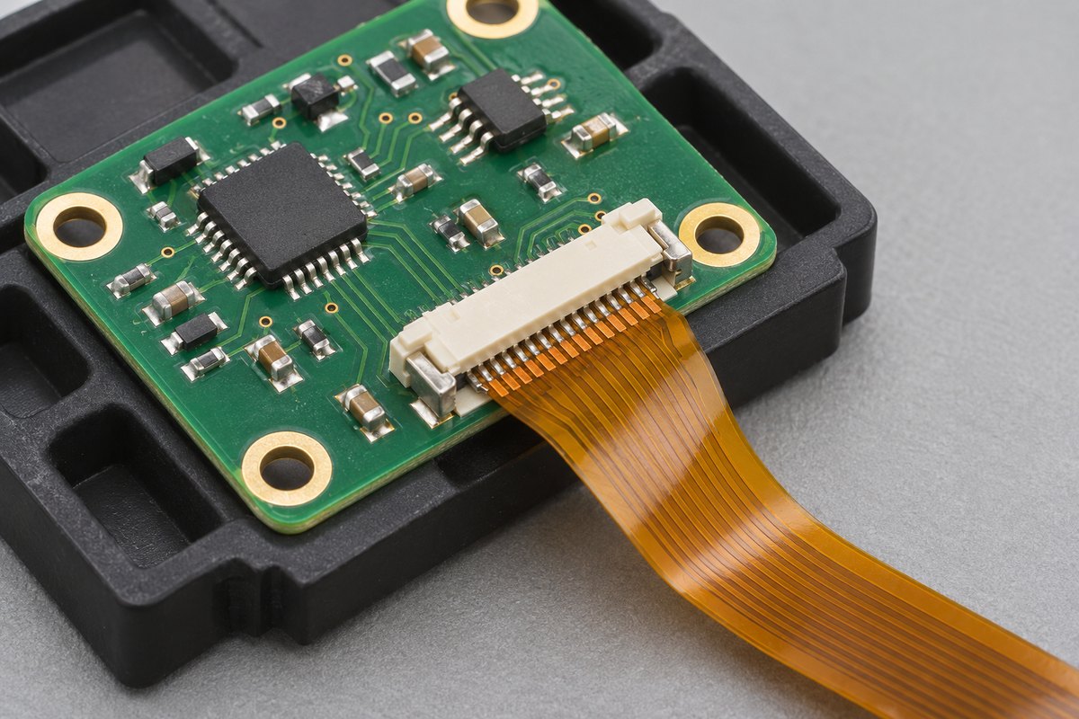
We provide strain gauge PCB assembly to customer-approved fabrication files, BOMs, and placement data. The scope can include component sourcing, PCB manufacture, component assembly, and agreed board-level testing.
Assembly planning addresses the following items:
- Component specifications: Preserve the specified resistor tolerances, amplifier grades, references, and other critical BOM requirements. Proposed substitutions require engineering approval rather than selection by package size alone.
- Flex support: Define assembly carriers and local reinforcement where needed to support flexible sections during placement and soldering.
- Process compatibility: Identify temperature-sensitive or cleaning-sensitive parts before choosing the soldering and cleaning processes.
- Test access: Include accessible power, ground, signal, and programming points for the agreed test procedure.
For a strain gauge sensor PCB, functional testing needs a defined input condition and acceptance limits. Sensor bonding, force fixtures, firmware loading, and calibration must each be identified in the assembly scope when required.
PCB Strain Gauge Testing vs. Standard PCB Inspection
PCB strain gauge testing measures mechanical strain on a board during a defined operation. Standard PCB inspection checks fabrication or assembly quality; it does not establish the board’s strain response or the accuracy of the completed sensor.
| Inspection or Test | Main Question Answered | Acceptance Basis |
|---|---|---|
| Bare-board electrical test | Are connections open or shorted? | Approved netlist |
| Dimensional and visual inspection | Does construction match the drawing? | Drawing and workmanship criteria |
| Assembly inspection | Are components and joints acceptable? | Assembly requirements |
| Functional test | Does the circuit respond correctly? | Agreed inputs and output limits |
| PCB strain gauge measurement | How does the board deform? | Defined operation and strain criteria |
Printed circuit board strain testing may be relevant to connector insertion, fixture loading, or other assembly operations. It requires suitable gauges, measurement equipment, mounting locations, and an agreed procedure. If your project requires this assessment, establish the testing responsibility and report requirements before production; it is not automatically included with ordinary PCB inspection.
For force-measurement electronics, board inspection and complete sensor calibration should also have separate acceptance criteria. A correct electrical connection alone cannot demonstrate measurement accuracy.
Prototype Strain Gauge Boards for Engineering Validation
We support prototype strain gauge boards and small production batches so your engineers can check the manufactured structure before committing to volume quantities. Prototype release should establish which revision and which physical features are being evaluated.
- Approve the manufacturing definition. Confirm the stackup, terminal thickness, outline, reinforcement, and assembly scope before fabrication.
- Evaluate the installation. Check connector engagement, flex routing, adhesive locations, and clearance inside the intended housing.
- Validate the circuit in its application. Use the selected sensor, electronics, and mechanical fixture to evaluate the complete measurement path.
- Freeze the production revision. Update the drawings, BOM, and acceptance criteria together so that the next batch reproduces the approved configuration.
Keep mechanical-fit changes separate from electrical changes in the revision record. This helps your team identify which modification produced a different result during validation.
Case Study: Flex Interconnect for a Strain Gauge Platform Sensor
A two-layer PI flex circuit we have manufactured provides a suitable interconnect structure for a strain gauge platform sensor. Its flexible routing section and reinforced attachment areas address the need to connect sensor terminals to a readout module within a restricted enclosure.
Application
In this arrangement, the sensing element remains on the force-bearing structure, while the FPC routes its connections to the electronics. The interconnect must fit around the internal structure without placing uncontrolled tension on the sensor terminations.
Manufacturing Challenges
- Different mechanical requirements: The routing section needs flexibility, while attachment areas need local support.
- Controlled attachment: Adhesive must follow defined locations without extending into the intended free-flex section.
- Edge quality: Sharp edges or burrs can interfere with handling and installation near other parts.
BestFPC Manufacturing Solutions
- Localized reinforcement: The board specification combines a two-layer PI circuit with FR4 stiffeners, concentrating support where the drawing requires it.
- Defined adhesive placement: 3M 966 adhesive is specified at drawing-defined locations to control attachment areas.
- Production drawing review: Stackup confirmation and edge-deburring requirements form part of the manufacturing definition before release.
Customer Benefits
This structure gives the engineer a thin routing section, reinforced mounting regions, and a defined attachment pattern to evaluate in the sensor assembly. It supports installation planning without requiring the flexible conductor itself to act as the sensing grid.
PCB Specifications
| Parameter | Board Specification |
|---|---|
| Circuit structure | Two-layer PI FPC |
| Board thickness | 0.23 mm |
| Coverlay | 50 µm, yellow |
| Local reinforcement | FR4 stiffeners |
| Attachment adhesive | 3M 966 at specified locations |
| Surface finish | ENIG |
| Legend | White |
| Edge requirement | Remove sharp edges and burrs |
How Quickly Can Strain Gauge PCBA Be Delivered?
Our quick-delivery PCBA option can support eligible projects in approximately 1.5 weeks, subject to material readiness, approved production files, and process requirements. The schedule for a strain gauge PCBA is confirmed against the actual build scope rather than applied automatically to every order.
- Material readiness: Long-lead amplifiers, connectors, or special materials can determine the earliest assembly date.
- Engineering release: Unresolved stackup, footprint, or mechanical questions must be closed before the production schedule is finalized.
- Test preparation: Custom fixtures, firmware, and calibration procedures may require preparation beyond the board build itself.
Confirm whether the quoted interval covers manufacturing only or also includes testing and dispatch. Transit time and customer-side installation are separate from the PCBA production schedule.
How Can Strain Gauge Circuit Board Costs Be Reduced?
Strain gauge circuit board costs can often be reduced by simplifying fabrication and sourcing while preserving the requirements that affect measurement and installation. Our DFM and BOM review helps identify which changes are worth evaluating before release.
- Use the necessary layer count: Additional layers should solve an identified routing or reference-plane requirement. Review simpler structures when the design permits them.
- Choose available material combinations: A standard PI and copper combination may avoid special procurement, provided it meets the approved mechanical and electrical requirements.
- Review panel utilization: Board shape, spacing, and assembly support requirements affect how efficiently a production panel can be used.
- Optimize component purchasing: Review availability and approved alternatives early. Do not trade away precision-component requirements solely for a lower unit price.
- Control revisions: Releasing coordinated fabrication and assembly files reduces the risk of purchasing parts or making tooling for an obsolete version.
Cost comparisons should use the same quantities, material specifications, test scope, and delivery conditions. Otherwise, a lower board price may simply exclude work included in another offer.
Why Choose BestFPC as Your Strain Gauge PCB Supplier?
BestFPC combines engineering review, PCB manufacturing, and assembly coordination to help OEM teams move from an approved design to a controlled production build. Our support focuses on the manufacturing decisions that affect your sensor integration and procurement process.
- Certified Quality Systems: Our qualifications include ISO 9001, ISO 13485, IATF 16949, and AS9100D. Applicable manufacturing-site and certification scope should match the order’s requirements; these management-system certifications do not replace finished-sensor qualification.
- Experienced Engineering Support: Our team includes R&D and PCB/PCBA engineers with 20 years of experience. DFM review reports and process recommendations give your engineers specific manufacturing issues to resolve before release.
- Integrated Manufacturing Resources: Our own PCB and PCBA factories, supported by more than 1,000 supply-chain partners, coordinate board production, component sourcing, and assembly through one project team.
- Development-Stage Support: Sample and small-batch production lets your team evaluate fit and integration before increasing order quantities.
- Digital Traceability: Our digital workshop supports retrieval of material and product-batch information, production-cycle details, and progress within five seconds, helping the project team investigate batch questions and track work status.
FAQs about Strain Gauge PCB
Can a copper PCB trace act as a strain gauge?
A copper trace changes resistance when it deforms, but that alone does not make it a qualified sensing element. A PCB trace strain gauge design needs its resistance, temperature response, geometry, and mechanical behavior evaluated. Treating a PCB trace as a strain gauge requires application validation rather than assuming that ordinary conductor specifications establish sensor performance.
Can a flex PCB combine constantan and copper?
Such a construction requires a separate material and process assessment. Provide the alloy specification, foil thickness, stackup, geometry, and required electrical properties. Standard PI/copper capability should not be used as confirmation that a constantan/copper stackup is production-ready.
Should the sensing grid and readout electronics use the same substrate?
That depends on the mechanical and electrical design. Separate structures allow the gauge to follow the force-bearing element while the electronics occupy a supported mounting area. Integration needs evaluation of strain transfer, component loading, and assembly processes.
Does PCB assembly include bonding the strain gauge to the test object?
Not automatically. Gauge bonding involves its own surface preparation, adhesive selection, placement, curing, and protection requirements. Define this operation separately from component assembly when discussing the project scope.
What connection details should be included for a bridge circuit?
Identify excitation, signal, and any sense connections in the schematic and connector pinout. State the applicable lead-resistance requirements and termination method so the interconnect and assembly drawings can be checked consistently.
Does a higher-resolution ADC guarantee better force accuracy?
No. Overall performance also depends on the sensor, excitation, analog circuitry, mechanical installation, temperature effects, and calibration. ADC resolution is one design parameter, not a complete accuracy specification.
For your next strain gauge PCB project, our engineering team can turn fabrication questions into a clear DFM review, coordinate approved BOM sourcing with PCB assembly, and support sample builds before volume production. These services help your team resolve manufacturing details while retaining control of sensor design and validation. Share your drawings and build requirements with sales@bestfpc.com to begin the review.


.png)
.png)
.png)
.png)

.png)