


 2025-09-23
 BEST
BEST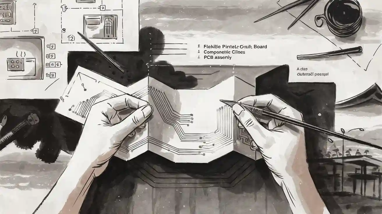
You fabricate a foldable PCB step by step by following a precise process that ensures durability and flexibility. Foldable PCBs use advanced materials and clever layouts to create circuits you can bend or fold without damage. These boards have transformed many industries, offering clear advantages over rigid alternatives.
- The flexible PCB market, which includes foldable types, reached USD 21.42 billion in 2023 and will likely grow to USD 61.75 billion by 2032, with a 12.52% annual growth rate.
| Industry/Application | Benefits of Flexible PCBs |
|---|---|
| Consumer Electronics | Ideal for compact devices like smartphones and wearables. |
| Automotive | Connects components in limited spaces, withstands vibrations. |
| Medical Devices | Lightweight and flexible for devices like pacemakers. |
| Aerospace and Defence | Critical for space-constrained applications in aircraft. |
| Industrial Automation | Durable in harsh environments with temperature extremes. |
| LED Lighting | Flexible connections for bendable lighting fixtures. |
For reliable foldable PCB fabrication, you must follow each step with care, as even small errors can affect performance. The benefits of flexible PCBs include space savings, resilience, and adaptability, but you face unique challenges throughout the process.
Key Takeaways
- Start with careful design and layout to manage mechanical stress and ensure flexibility in foldable PCBs.
- Select the right materials, like polyimide, for optimal durability and performance in flexible circuit applications.
- Follow precise lamination and layer bonding techniques to create strong and reliable foldable PCBs.
- Conduct thorough testing and quality control to verify the performance and reliability of your foldable PCBs.
- Avoid common mistakes, such as ignoring bend radius and material compatibility, to enhance the longevity of your designs.
Foldable PCB Fabrication Steps
Design & Layout
You begin foldable PCB fabrication with design and layout creation. This stage sets the foundation for reliable flex circuit boards. You must address unique mechanical and electrical requirements. Unlike rigid boards, flex circuit design demands careful management of mechanical stress, bend radius, and integration of flexible and rigid sections.
| Design Consideration | Foldable PCBs | Rigid PCBs |
|---|---|---|
| Mechanical Stress Management | Critical due to bending | Less critical |
| Bend Radius Limitations | Must adhere to specific limits | Not applicable |
| Integration of Sections | Requires careful design | Standard layout |
You need to tailor Design Rule Checks (DRC) for both electrical and mechanical constraints. Neglecting these factors can cause cracked traces or board failure. Professional CAD tools offer advanced features such as multi-zone layer management, dynamic bending simulations, and automated routing for flex areas. Open-source and cloud-based platforms provide basic support and collaboration features. You should use DFM checks, bend radius calculation software, and material databases to optimise your design.
Tip: Always simulate bending stress and check trace spacing before moving to fabrication.
Material Selection
Material selection is crucial in flexible PCB production. You must choose substrates that balance flexibility, durability, and electrical performance. Polyimide stands out for its exceptional flexibility and high dielectric strength, making it ideal for repeated bending. Polyester (PET) offers moderate flexibility and cost-effectiveness, suitable for consumer electronics. PTFE provides chemical resistance and low dielectric constant, essential for aerospace and automotive applications.
| Material | Mechanical Properties | Electrical Properties |
|---|---|---|
| Polyimide | Exceptional flexibility, high dielectric strength | Good electrical properties, heat resistance |
| Polyester (PET) | Moderate flexibility, cost-effective | Moderate heat and chemical resistance |
| PTFE | Exceptional chemical resistance, low friction coefficient | Low dielectric constant, low dissipation factor |
The choice of substrate directly impacts the flexibility and durability of flex circuit boards. Polyimide offers high mechanical strength, while polyester is less durable in harsh environments. Liquid crystal polymer provides moisture resistance and high-frequency performance. Thinner circuits bend more easily but may lose durability over time.
Lamination & Layer Bonding
Lamination and layer bonding give flex circuit boards their structure. You prepare layers by cutting copper foil and polyimide films, then align them using optical registration systems. You apply controlled heat and pressure to activate adhesives and bond layers. Polyimide coverlay adds insulation and flexibility.
| Lamination Type | Description |
|---|---|
| Standard Rigid PCB Lamination | Presses layers of prepreg with copper foil at high temperature. |
| Multilayer PCB Lamination | Stacks multiple copper layers, requiring precise alignment. |
| Flexible PCB Lamination | Uses polyimide films and ultra-thin copper foil, with lower pressure and temperature. |
| Rigid Flex PCB Lamination | Combines rigid and flexible materials for high-performance electronics. |
You must mitigate challenges such as mismatched material properties and structural discontinuity. Use symmetrical stack-ups, adhesive-less PI substrates, and staged temperature profiles to ensure balanced stress and dimensional stability.
Note: Pre-treat materials to remove moisture and use pressure equalisation materials for even bonding.
Circuit Patterning
Circuit patterning defines the electrical pathways on flex circuit boards. You use photolithography to apply photoresist and etch circuit patterns. Digital imaging with computer-controlled lasers enables precise placement. Lamination and curing secure the layers, while drilling creates holes for electrical connections.
| Technique | Description |
|---|---|
| Photolithography | Cleans substrate, applies photoresist, uses photomask to etch patterns. |
| Digital Imaging | Uses lasers for precise circuit patterning. |
| Lamination | Bonds flexible layers with adhesive under heat and pressure. |
| Curing | Hardens adhesive using UV, thermal, or microwave methods. |
| Drilling | Creates holes for electrical connections. |
| Plating Techniques | Through-hole plating, electroplating, vertical continuous plating for interconnections. |
Drilling
Drilling forms vias and holes for component mounting and interconnections. You use laser drilling for precision, achieving hole sizes as small as 25 micrometres. Careful drilling prevents damage to delicate materials. Misalignment or oversized vias can disrupt signal paths and compromise board integrity. Advanced CNC equipment ensures tight tolerances.
- Laser drilling enables high precision for flex circuit boards.
- Proper alignment and size control are essential for reliable flexible PCB production.
Copper Plating
Copper plating creates conductive pathways and interconnects. You start by drilling and cleaning the substrate. Pre-treatment, such as electroless copper or the Black Hole process, enhances adhesion. Electroplating deposits copper onto prepared surfaces, with thickness controlled for electrical and mechanical needs. A photo-imaged resist defines the circuit pattern, ensuring copper only covers designated areas.
- Drilling and cleaning
- Pre-treatment for adhesion
- Electroplating process
- Photo-imaged circuit pattern
- Inspection and quality control
You must optimise copper thickness to balance flexibility and conductivity. Fine-pitched patterns allow precise control, and layered structures must remain platable without delaminating.
Dry Film Lamination
Dry film lamination protects and insulates circuit patterns. You use base films such as polyimide for thermal stability or polyester for cost-sensitive applications. Epoxy adhesives offer semi-cured stability, while acrylic adhesives provide longer shelf life and require higher lamination temperatures.
| Material Type | Description |
|---|---|
| Base Film | Polyimide (PI) for thermal stability; polyester (PET) for cost-sensitive applications. |
| Adhesive Types | Epoxy: Semi-cured, 3–4-month shelf life at 5°C; Acrylic: Stable, >6-month shelf life, higher lamination temperature (160–200°C). |
You must select adhesives and films that match your application's thermal and mechanical requirements.
Etching
Etching removes unwanted copper, leaving behind fine circuit features. Chemical etching achieves minimum trace and space widths of 0.2mm, offering medium-high reliability and fast processing. CNC milling provides wider traces but takes longer and offers lower reliability.
| Parameter | CNC Milling | Chemical Etching |
|---|---|---|
| Minimum Trace / Space | 0.4mm/0.4mm | 0.2mm/0.2mm |
| Reliability | Low | Medium-High |
| Time to Etch One PCB | 10-40+ minutes | ~4 minutes |
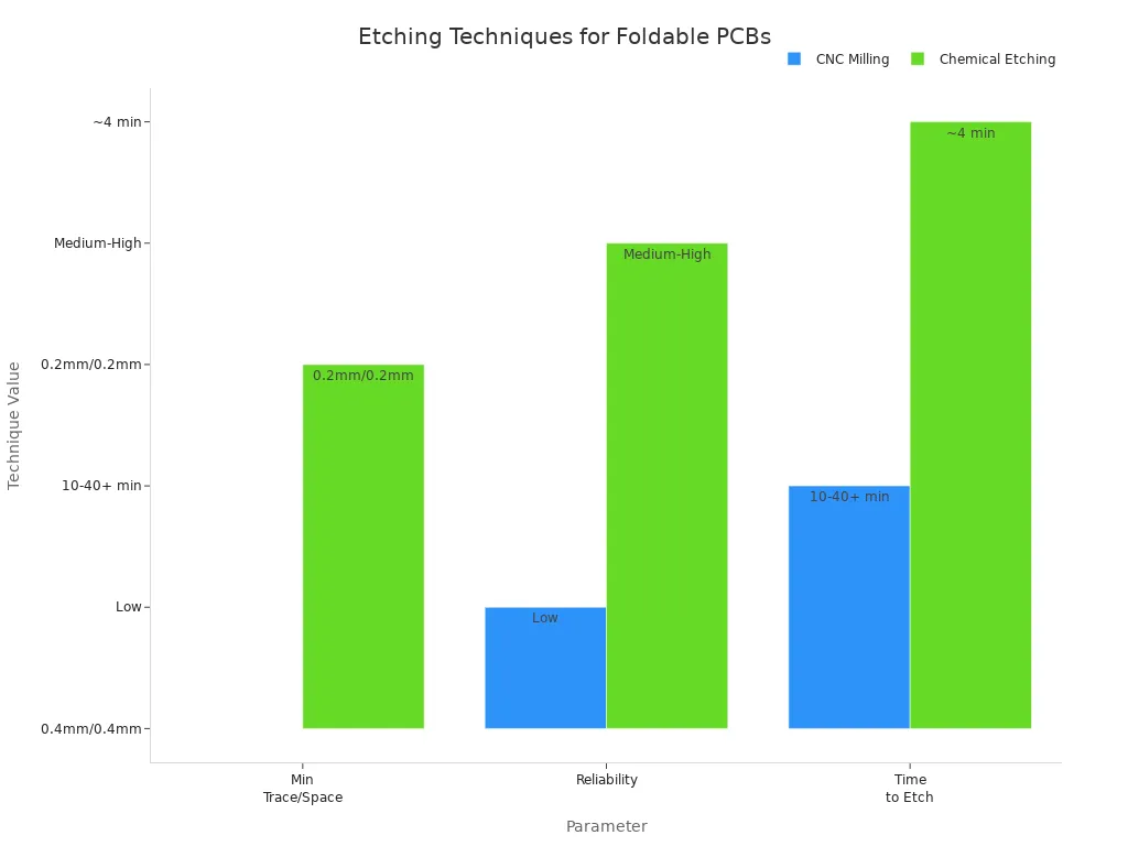
Chemical etching is preferred for flexible PCB production due to its speed and precision.
Assembly
Assembly places and secures components on flex circuit boards. You must minimise stress during reflow and avoid sharp bends. Use solder paste, adhesive dots, or hot-melt studs for larger components. Vision systems ensure accurate placement, and temperature control prevents excessive pressure. Nitrogen atmospheres reduce oxidation, while vacuum tables prevent shifting or warping.
| Assembly Method | Key Considerations |
|---|---|
| Component Placement | Minimise stress during reflow; avoid sharp bends. |
| Mechanical Attachments | Use solder paste, adhesive dots, or hot-melt studs for larger components. |
| Placement Accuracy | Use vision systems for alignment. |
| Temperature Control | Gentle temperature ramps; lower peak temperatures. |
| Inert Atmosphere | Nitrogen prevents oxidation. |
| Secure Fixtures | Vacuum tables prevent shifting. |
| Bending Radius | Maintain proper radius during soldering. |
| Inspection and Testing | Rigorous checks for reliability. |
You must maintain the correct bending radius during soldering to avoid damage.
Testing
Testing verifies the electrical and mechanical performance of foldable PCB fabrication. You use protocols such as IPC-2223 for reliability under bending and high voltage. IPC-A-600 sets visual inspection criteria for defects. IPC-TM-650 provides methods for peel strength and HiPot testing. IPC-TM-650 2.6.7 assesses thermal shock resistance, while IPC-TM-650 2.5.5.7 uses TDR impedance testing for signal quality. IPC-6013 outlines qualification requirements, and IPC-TM-650 Method 2.4.3 details flexural endurance testing.
| Testing Protocol | Description |
|---|---|
| IPC-2223 | Evaluates electrical and mechanical reliability under bending and high-voltage exposure. |
| IPC-A-600 | Sets visual inspection criteria for cracks or delamination. |
| IPC-TM-650 | Methods for peel strength and HiPot testing. |
| IPC-TM-650 2.6.7 | Assesses thermal shock resistance. |
| IPC-TM-650 2.5.5.7 | TDR impedance testing for signal quality. |
| IPC-6013 | Qualification and performance requirements for flex PCBs. |
| IPC-TM-650 Method 2.4.3 | Flexural endurance testing for mechanical durability. |
You must conduct rigorous inspection and testing to ensure reliability and performance in flexible PCB production.
Flexible PCB Manufacturing Materials
Substrate Options
You must select the right substrate to achieve reliable flexible pcb manufacturing. The substrate forms the backbone of flex circuit boards, influencing flexibility, thermal stability, and electrical performance. Polyimide stands out as the most popular choice for flexible pcb production. You benefit from its high thermal resistance, low moisture absorption, and excellent flexural strength. Polyester (PET) offers a cost-effective alternative, suitable for less demanding environments. Liquid Crystal Polymer (LCP) and PTFE provide superior performance for high-frequency and aerospace applications. Adhesiveless substrates deliver enhanced flexibility and durability, especially in dynamic bending scenarios.
| Property | Polyimide | Polyester (PET) | LCP | PTFE | Adhesiveless |
|---|---|---|---|---|---|
| Thermal Resistance | Up to 260 °C | Up to 120 °C | Up to 200 °C | Up to 250 °C | Up to 240 °C |
| Dielectric Constant | 3.4 @1 MHz | 3.2 @1 MHz | 2.9 @1 GHz | 2.1 @10 GHz | 3.5 @1 MHz |
| Dissipation Loss (tan δ) | 0.0025 @1 MHz | 0.02 @1 MHz | 0.0015 @1 GHz | 0.0004 @10 GHz | 0.003 @1 MHz |
| Flexural Strength | 120 MPa | 80 MPa | 100 MPa | 90 MPa | 130 MPa |
| Moisture Absorption | 0.5 % | 0.3 % | 0.02 % | 0.01 % | 0.4 % |
| Typical Thickness Range | 12–75 µm | 25–125 µm | 50–150 µm | 25–100 µm | 12–50 µm |
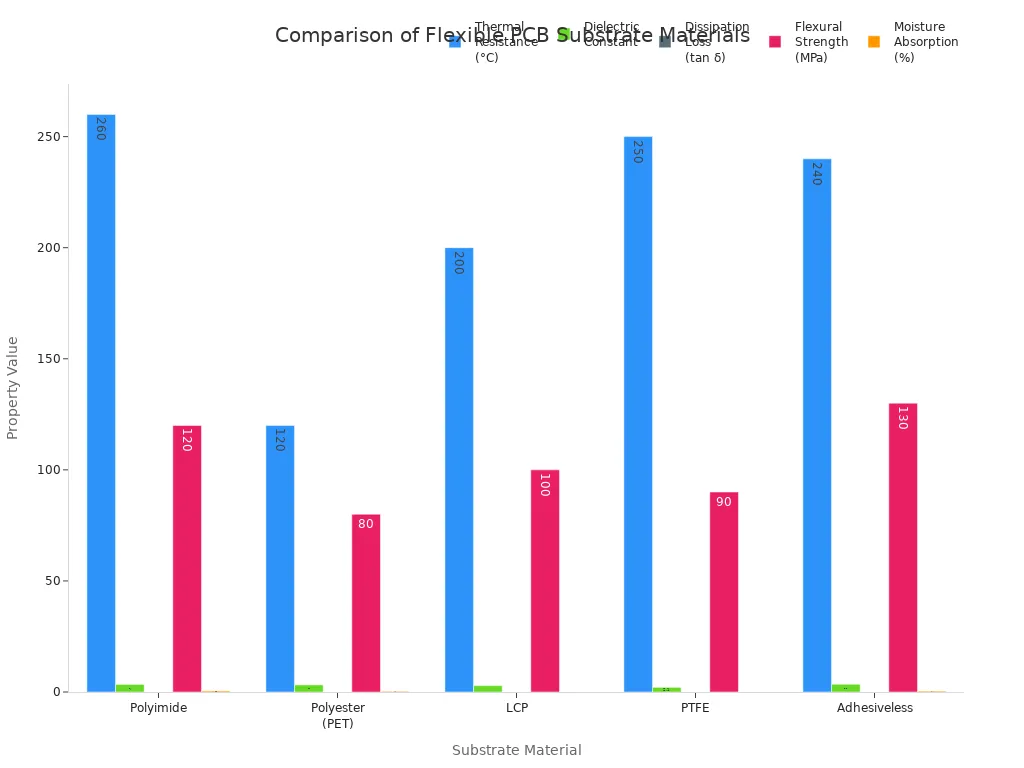
Tip: You should choose polyimide for most flexible pcb manufacturing projects. It offers a balance of heat resistance and mechanical strength. For high-frequency circuits, LCP and PTFE substrates minimise signal loss.
Conductive Layers
You need to select conductive materials that match your application and performance goals. Copper remains the standard for flex circuit boards due to its conductivity and ductility. You can use rolled annealed copper for enhanced flexibility in dynamic folding. For flexible pcb production in high-frequency environments, you should consider materials like Rogers 4003c, which reduce signal loss and maintain integrity.
- Polyimide and polyester substrates support copper layers, allowing repeated bending without cracking.
- Dupont's "Kapton" polyimide film provides heat resistance and dimensional stability, with a low dielectric constant that benefits signal performance.
- High-frequency materials such as Rogers 4003c ensure minimal signal degradation in advanced flexible pcb manufacturing.
You must ensure the conductive layer thickness matches your design requirements. Thinner copper layers improve flexibility, while thicker layers support higher current loads.
Note: Always verify compatibility between substrate and conductive layers to prevent delamination and maintain long-term reliability.
Quality Control in Foldable PCB Fabrication
Automated Optical Inspection
You must use automated optical inspection (AOI) to maintain high standards in flexible pcb production. AOI systems scan flex circuit boards with high-resolution cameras, detecting defects such as misaligned components, solder bridges, and broken traces. The technology achieves a defect detection accuracy of 99.5%, which far exceeds manual inspection rates. You position AOI checkpoints at several stages during assembly, ensuring early identification of flaws. The camera resolution, often 10μm/pixel, allows you to spot even the smallest imperfections. AOI supports your testing and quality assurance process by providing rapid feedback and reducing the risk of faulty boards reaching customers.
AOI not only improves reliability but also speeds up inspection, helping you deliver consistent quality in flexible pcb production.
Quality control standards play a vital role in certifying flex circuit boards. You must comply with recognised certifications to meet industry expectations.
| Quality Control Standards and Certifications | Description |
|---|---|
| ISO 9001:2008 | Quality management systems standard. |
| ISO 14001:2004 | Environmental management systems standard. |
| ISO/TS 16949:2009 | Quality management standard for automotive production. |
| UL | Safety certification for products. |
Reliability Testing
Reliability testing ensures your flex circuit boards withstand repeated bending and environmental stress. You perform bend cycle tests, simulating thousands of folding and unfolding actions to check durability. Tensile and compression tests measure mechanical strength, while thermal cycling exposes boards to extreme temperatures. Humidity and environmental tests assess performance under high moisture conditions. Electrical reliability tests confirm that signal integrity remains stable after mechanical stress.
| Testing Method | Objective | Key Parameters |
|---|---|---|
| Bend Cycle Testing | Simulate repeated bending and unfolding to evaluate durability | Bend radius (2 mm, 5 mm, 10 mm), Number of cycles (10,000 to 100,000), Bending angle (180°, 360°) |
| Tensile and Compression Testing | Evaluate mechanical strength under tensile and compressive forces | Force applied, Material deformation and failure points |
| Thermal Cycling Testing | Assess impact of temperature variations on mechanical reliability | Temperature range (-40°C to +85°C), Number of cycles (1,000 to 5,000) |
| Humidity and Environmental Testing | Evaluate impact of humidity and environmental factors | Humidity levels (85% RH at 85°C), Duration of exposure (1,000 hours) |
| Electrical Reliability Testing | Assess impact of mechanical stress on electrical performance | Resistance measurements before and after testing, Signal integrity and continuity checks |
You must follow strict procedures for testing and quality assurance. Full inspection by your QA team, regular calibration of equipment, and internal audits help you maintain consistent standards in flexible pcb production. Certified boards bear the UL Recognised Component Mark and include detailed documentation.
You should always prioritise reliability testing to guarantee long-term performance and safety for your flex circuit boards.
Common Challenges
Cracks & Delamination
You often face cracks and delamination during foldable PCB fabrication. These issues arise when you expose the board to repeated bending or mechanical stress. Improper component placement and environmental factors, such as moisture absorption, also contribute to failures.
- Mechanical stress from bending weakens the substrate.
- Placing components in bending zones increases risk.
- Moisture absorption leads to delamination over time.
To prevent these problems, you should design with care and place components away from areas that bend. Flexible adhesives around solder joints help absorb stress. Stiffeners under critical components add support. Polyimide substrates with low moisture absorption offer better durability. You can apply conformal coatings or protective coverlays to shield the board from moisture and chemicals.
Tip: Always inspect for early signs of cracks and delamination during quality control.
Bending Radius
You must calculate the correct bending radius to avoid damaging your foldable PCB. The minimum recommended bending radius depends on the number of layers and whether the design is stable or dynamic. Use the formula: Minimum bending radius = (r/h of design standard) × application thickness. This calculation helps you determine how much the board can bend safely.
| Layer | Stable Design | Dynamic Design |
|---|---|---|
| Single Layer | 10:1 | 100:1 |
| Double Layer | 10:1 | 150:1 |
| Multi-layer | 20:1 | Not recommended |
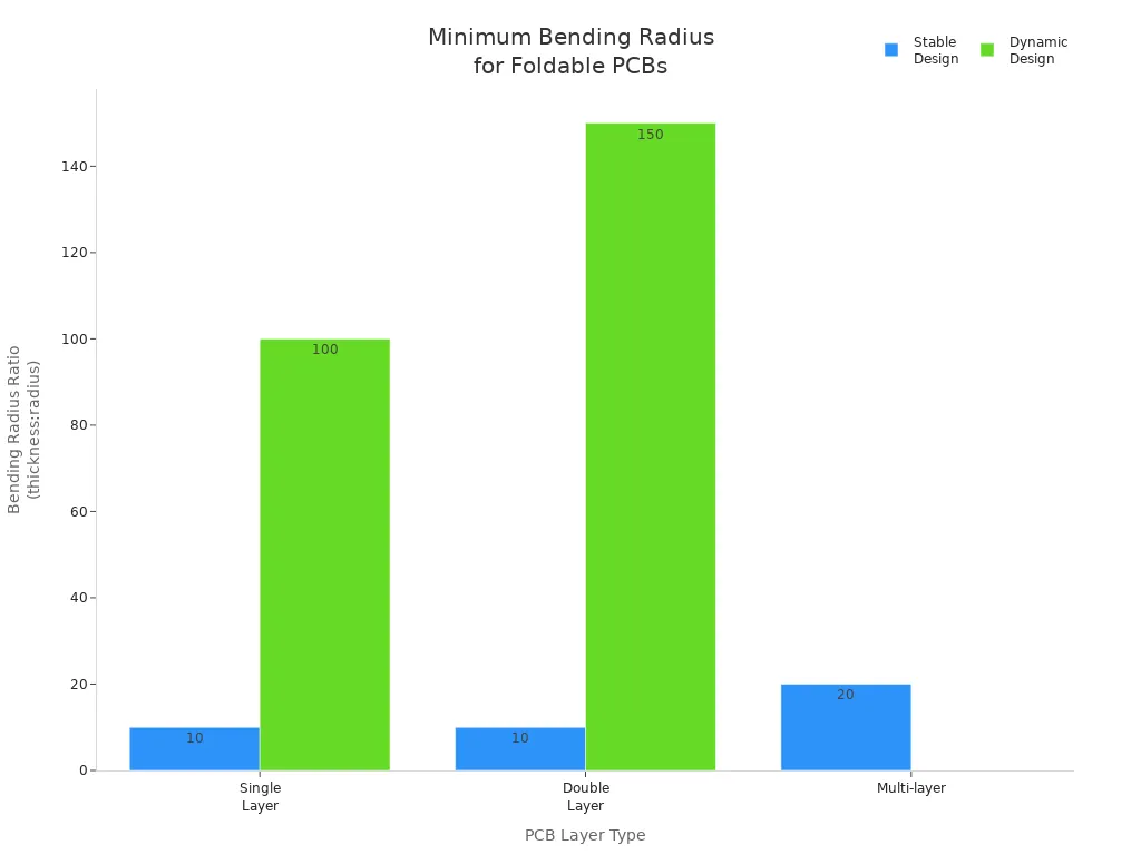
You should avoid multi-layer designs for dynamic bending applications. Always check the material properties before finalising your design.
Long-term Reliability
You need to consider several factors to ensure long-term reliability in foldable PCBs, especially in consumer electronics. Material selection plays a key role. The right substrate and conductive materials improve durability. Proper design, including bend radius and trace layout, maximises reliability. Quality control during manufacturing prevents defects that shorten lifespan. Environmental conditions, such as temperature extremes and moisture, affect performance. Mechanical stress from repeated bending and vibration remains a primary cause of failure.
| Factor | Description |
|---|---|
| Material Selection | The choice of substrate and conductive materials affects durability. |
| Design Considerations | Proper bend radius and trace layout maximise reliability. |
| Manufacturing | Quality control prevents defects and extends lifespan. |
| Environment | Temperature, moisture, and chemicals impact performance. |
| Mechanical Stress | Repeated bending and vibration cause failures in flexible circuits. |
You must address the challenges of flex pcb manufacturing by combining careful design, robust material selection, and thorough testing. These steps help you achieve reliable and long-lasting foldable PCBs.
Tips for Success
Best Practices
You can achieve reliable results in foldable PCB projects by following industry-recommended best practices. These steps help you avoid common pitfalls and improve both performance and durability:
- Select the right materials. Choose substrates such as polyimide for high thermal resistance and rolled annealed (RA) copper for dynamic applications.
- Optimise the bend radius for reliability. Calculate the minimum bend radius based on the number of layers to prevent fatigue fractures.
- Design traces for flexibility and signal integrity. Use hatched polygons and staggered traces to enhance flexibility and maintain signal quality.
- Incorporate stiffeners for mechanical support. Add stiffeners in critical areas to prevent damage from repeated bending.
- Collaborate with fabricators early. Engage with manufacturers during the design phase to ensure compatibility and reduce costs.
- Test for reliability and compliance. Conduct tests to meet IPC standards and ensure durability in demanding environments.
Following these tips for successful flexible pcb fabrication will help you deliver robust and long-lasting products.
Mistake Prevention
You can prevent costly errors by recognising common mistakes and applying proven solutions. The table below outlines frequent issues and how you can address them:
| Common Mistakes | Solutions |
|---|---|
| Ignoring Minimum Bend Radius | Maintain a bend radius of at least 6× board thickness for static use. Use 100× thickness for dynamic flexing. |
| Poor Material Selection and Stackup | Use polyimide substrates for high-temperature resilience. Avoid PET in high-heat applications. |
| Overlooking Connector Compatibility | Ensure connector pitch matches trace spacing. Use ZIF or LIF connectors to reduce insertion pressure. |
| Underestimating High-Speed Signal Challenges | Apply controlled impedance rules. Embed ground planes and keep trace geometry consistent. |
| Skipping Environmental Protection | Apply conformal coatings to shield against contaminants. Bake out boards to remove moisture. |
| Design for Test and Manufacturability | Include test points and perform pre-production checks for electrical validation. |
You should always review your design and process steps to catch these issues early. This approach saves time and ensures higher reliability.
You achieve reliable foldable PCB fabrication by following each step with precision. Careful design, robust material selection, and strict process control ensure durability and performance.
For best results, you should:
- Handle flexible circuits with clean gloves and store them flat.
- Avoid sharp bends and inspect for defects before assembly.
- Prepare your workspace to prevent static discharge.
.png)
.png)
.png)
.png)

.png)

