


 2026-11-04

 BEST
A hybrid rigid-flex PCB connects rigid component areas through flexible circuits, making it possible to fit complex electronics into compact, three-dimensional enclosures. The challenge is getting the stackup right. Too many copper layers in the flexible section can increase stiffness, limit the bend radius, and complicate assembly. A six-layer rigid section, for example, may need only two layers through the bend.
BestFPC provides custom hybrid rigid-flex PCB fabrication, free DFM review, prototyping, and assembly services. From mixed-layer stackups to HDI interconnections, we help customers evaluate materials, mechanical requirements, and manufacturing feasibility before production. This guide covers the construction options, design rules, and manufacturing considerations that matter when planning a hybrid rigid-flex PCB.
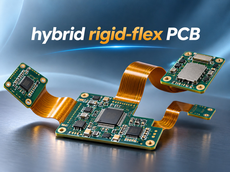
What Is a Hybrid Rigid-Flex PCB, and When Should You Use One?
A hybrid rigid-flex PCB combines rigid component-mounting sections with flexible electrical connections in a single board. The rigid areas support components and connectors, while the flexible sections allow circuits to occupy different positions within an enclosure.
The term "hybrid" generally describes this combination. It may also refer to designs with different materials, regional layer counts, or asymmetric stackups. It is not a separate standardized PCB category.
Hybrid rigid-flex construction is worth considering when:
-
Installation space is limited: Several rigid circuit areas must fit into a compact or irregular enclosure.
-
Connectors add complexity: Integrated flexible connections can replace separate cables and board-to-board connectors.
-
Routing requirements differ: Rigid sections need additional signal or reference layers that are unnecessary in the flexible regions.
-
The assembly requires folding: Circuit sections must occupy different planes without losing electrical continuity.
A conventional rigid PCB with a separate flexible cable may be more economical for a simple connection. Hybrid rigid-flex PCB construction becomes more attractive when integrated packaging, reduced connector count, or complex routing provides a clear advantage.
Where Are Hybrid Rigid-Flex PCBs Used in Electronic Products?
Hybrid rigid-flex PCBs are commonly used where components must remain mechanically supported while electrical connections pass through narrow or curved spaces.
-
Medical Electronics: Portable diagnostic instruments and monitoring equipment can connect sensor modules and control circuits within compact housings.
-
Wearable Electronics: Smartwatches and body-worn sensors use flexible connections to accommodate curved enclosures and closely positioned components.
-
Automotive Electronics: Camera modules and sensor assemblies can integrate circuits mounted at different angles while reducing internal connectors.
-
Industrial Electronics: Machine-vision systems and precision instruments can connect multiple rigid circuit sections within space-constrained equipment.
-
Aerospace Electronics: Compact avionics modules may use integrated rigid-flex circuits to reduce interconnection hardware and accommodate complex mechanical layouts.
For these products, the important distinction is whether the flexible section bends only during installation or moves repeatedly throughout operation. Dynamic bending requires a different material and mechanical design approach from a one-time fold.
Which Stackup Structures Are Practical for Hybrid Rigid-Flex PCBs?
Hybrid rigid-flex PCB stackups can use different copper layer counts in rigid and flexible sections. This allows higher routing density around components without making every conductive layer part of the bending structure.
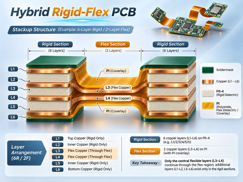
Consider a 6-layer rigid / 2-layer flex construction. In one possible arrangement, L1, L2, L5, and L6 exist only in the rigid regions, while L3 and L4 form a continuous flexible core. This provides additional routing layers around components while keeping the flexible connection relatively thin.
| PCB Structure | Rigid / Flex Layers | Typical Design Requirements |
|---|---|---|
| 4-Layer Hybrid Rigid-Flex PCB | 4 / 2 | Compact assemblies with moderate routing density |
| 6-Layer Hybrid Rigid-Flex PCB | 6 / 2 | Additional rigid-region routing with a thin flex connection |
| 8-Layer Hybrid Rigid-Flex PCB | 8 / 2 | Dense component areas with fewer layers through the bend |
| 8-Layer Hybrid Rigid-Flex PCB | 8 / 4 | More signals or reference conductors required in flexible regions |
| HDI Hybrid Rigid-Flex PCB | Custom | Fine-pitch components, microvias, and complex interlayer connections |
These are representative constructions. The final arrangement must account for layer continuity, copper thickness, dielectric materials, and the required mechanical geometry.
For controlled-impedance circuits, the flexible section must retain suitable return paths. Removing copper layers simply to reduce thickness can create signal-integrity problems if the resulting reference-plane arrangement is inadequate.
Which Materials Should You Choose for Rigid and Flexible Sections?
Hybrid rigid-flex PCB construction typically combines FR-4 rigid laminates with polyimide-based flexible circuits. Copper type, bonding materials, and dielectric thickness influence both electrical performance and bending behavior.
-
FR-4: Provides mechanical support for components and multilayer circuitry. The selected grade must meet the required thermal and electrical conditions.
-
Polyimide (PI): Forms the flexible dielectric. Thinner PI can reduce the overall flex thickness, provided the construction meets electrical and mechanical requirements.
-
Rolled Annealed (RA) Copper: Often preferred for applications involving repeated bending because of its ductility and fatigue characteristics.
-
Electrodeposited (ED) Copper: Suitable for rigid circuitry and certain static-flex constructions, depending on the selected foil and bend conditions.
-
Adhesiveless Laminates: Eliminate the conventional adhesive layer between copper and the PI core, allowing thinner flexible constructions.
-
Low-Flow Prepreg: Bonds rigid and flexible materials while helping prevent unwanted resin flow into exposed flex areas.
-
Polyimide Coverlay: Protects flexible conductors and provides openings for contacts and solder connections.
Copper thickness deserves particular attention. Increasing copper weight may improve current capacity, but it also makes the flexible section harder to bend. Where the stackup permits, different copper specifications can be used in rigid and flexible regions.
The selected materials must also withstand the planned lamination and assembly temperatures without compromising layer adhesion or dimensional stability.
What Are the Critical Design Rules for a Hybrid Rigid-Flex PCB?
A hybrid rigid-flex PCB must work electrically when flat and remain reliable after installation. Bend geometry, conductor routing, and rigid-to-flex transitions should therefore be checked alongside the electrical layout.
| Design Item | Reference or Requirement | Design Recommendation |
|---|---|---|
| Static Bend, 1–2 Flex Layers | Approximately 10× finished flex thickness as an initial guideline | Confirm the radius using the complete flex construction |
| Static Bend, 3+ Bonded Flex Layers | Approximately 20× finished flex thickness as an initial guideline | Reduce bonded flex layers if bending space is restricted |
| Dynamic Bend, 1 Flex Layer | Approximately 100× flex thickness as a preliminary reference | Select suitable copper and verify the required bending cycles |
| Dynamic Bend, 2 Flex Layers | Approximately 150× flex thickness as a preliminary reference | Confirm fatigue performance under actual operating conditions |
| Rigid-to-Flex Transition | Clearance depends on the approved construction | Keep stress-sensitive features away from the transition and active bend |
| Trace Routing | Conductors should cross the bend axis approximately perpendicular to it | Avoid sharp corners and sudden trace-width changes |
| Copper Distribution | Determined by electrical and mechanical requirements | Limit unnecessary solid copper in active bend regions |
| Controlled Impedance | Depends on dielectric properties, trace geometry, and reference planes | Evaluate rigid and flexible transmission-line structures separately |
| Mechanical Fit | Bend angle, radius, direction, and installed clearance must be defined | Check the folded assembly using a mechanical drawing or 3D model |
Bend-radius multipliers are starting references rather than guaranteed manufacturing limits. IPC-2223 design guidance, the actual material construction, and the expected bending conditions should determine the final specification.
A design intended for continuous movement must also consider the number of bending cycles. Static-flex construction should not be assumed to withstand repeated movement without qualification.
How Should You Plan Vias and BGA Fanout in a Hybrid Rigid-Flex PCB?
Via selection depends on the layer connections required, component pitch, and available routing area. A hybrid rigid-flex PCB does not automatically require HDI technology; conventional plated through-holes remain practical where routing space permits.
-
Plated Through-Holes: Connect conductive layers through suitable rigid sections and are generally preferred when component density allows.
-
Blind Vias: Connect an external layer to selected internal layers without passing through the entire stackup.
-
Buried Vias: Connect internal layers and are usually formed before final lamination.
-
Laser Microvias: Provide short connections between adjacent layers for fine-pitch BGA fanout and dense HDI routing.
For example, a fine-pitch BGA on a six-layer rigid section may not have enough space for conventional through-hole escape routing. Laser microvias can connect selected BGA pads to the next routing layer, while additional connections use an approved combination of microvias and internal vias.
Via-in-pad structures may require filling and capping to produce a suitable soldering surface. Stacked microvias also require review because they introduce additional manufacturing and reliability considerations.
Keep plated vias outside active bending regions. Conductors passing between rigid sections should follow the continuous copper layers specified in the flexible core.
How Is a Hybrid Rigid-Flex PCB Fabricated?
Hybrid rigid-flex PCB manufacturing combines flexible circuit processing with multilayer PCB fabrication. The sequence changes according to the stackup, particularly when buried vias or sequential lamination are required.
The main production stages are:
-
Engineering Review: Verify fabrication files, layer continuity, materials, via structures, bend requirements, and critical tolerances.
-
Flexible Circuit Fabrication: Form copper circuits on PI substrates and apply the specified coverlay.
-
Rigid Inner-Layer Processing: Produce rigid circuit layers and complete internal interconnections that must be formed before final lamination.
-
Rigid-Flex Lamination: Align and bond rigid and flexible materials while controlling registration, resin flow, and bonding conditions.
-
Drilling and Metallization: Form plated holes and other interconnections using the approved drilling and copper-plating processes.
-
Outer-Layer Processing: Complete external circuitry and apply the required surface finish.
-
Profiling and Inspection: Form the board outline and flex openings, inspect critical dimensions, and perform electrical testing.
Depending on the product requirements, inspection can include cross-section analysis, controlled-impedance verification, and bending tests.
For complex constructions, engineering approval of the stackup and drilling sequence before fabrication helps avoid changes after the circuit layout has been finalized.

What Affects Hybrid Rigid-Flex PCB Cost and Lead Time?
Hybrid rigid-flex PCB cost and lead time depend on the complete construction, not simply the number of copper layers. A six-layer design requiring sequential lamination and several microvia structures can involve more processing than a conventional eight-layer stackup.
The main factors are:
-
Stackup Complexity: Regional thickness differences and additional lamination cycles increase processing requirements.
-
HDI Features: Blind vias, buried vias, and laser microvias may add drilling, plating, and inspection operations.
-
Materials: Specialty laminates, copper foils, and bonding materials affect procurement and manufacturing planning.
-
Board Geometry: Irregular outlines and multiple flexible sections influence panel utilization.
-
Order Quantity: Prototypes, small batches, and production orders have different setup and scheduling requirements.
-
Testing: Additional mechanical qualification, impedance verification, or documentation can extend the manufacturing schedule.
Cost can often be reduced by using available materials, avoiding unnecessary copper layers in flexible regions, and choosing simpler via structures where the routing permits. Panel utilization is also worth reviewing before the board outline is finalized.
Lead time should be confirmed after the stackup, material requirements, quantity, and testing scope have been reviewed. Manufacturing time should be distinguished from shipping and customs clearance.
Why Choose BestFPC for Hybrid Rigid-Flex PCB Manufacturing?
BestFPC provides custom hybrid rigid-flex PCB fabrication, engineering support, and assembly services. From complex stackups to volume production, we help customers turn challenging designs into manufacturable PCB solutions.
-
Free DFM and Engineering Support: Get professional feedback on stackup design, bend radius, rigid-to-flex transitions, and via placement before fabrication, reducing costly design changes and production risks.
-
Custom Stackup and Material Solutions: Choose from different rigid/flex layer configurations, FR-4, polyimide, and suitable copper materials. Our engineers help you select a construction that meets your electrical and mechanical requirements.
-
Advanced Multilayer Manufacturing: Access 2–20-layer rigid-flex PCB manufacturing capabilities, including fine-line circuitry and applicable HDI structures. Complex designs are reviewed to confirm achievable specifications before production.
-
Prototype to Volume Production: Start with engineering samples to verify electrical performance and mechanical fit, then move to small-batch or volume production using approved materials and manufacturing specifications.
-
One-Stop PCB Fabrication and Assembly: Reduce supplier coordination by combining PCB manufacturing, component sourcing, SMT assembly, and applicable testing services within one project.
-
Quality Assurance and Traceability: Benefit from ISO 9001 and ISO 13485 quality management systems, electrical testing, manufacturing inspections, and project-specific quality documentation.
-
Reliable Engineering Communication and Lead Time: Receive technical feedback on manufacturing feasibility, material availability, and production requirements, along with a project-specific quotation and lead time.
Frequently Asked Questions About Hybrid Rigid-Flex PCBs
Q1: Can a hybrid rigid-flex PCB have multiple independent flexible tails?
A1: Yes. Several flexible sections can connect different rigid areas. Each tail must have defined dimensions, layer continuity, and bending requirements.
Q2: Can FR-4 or PI stiffeners be added beneath flexible connector contacts?
A2: Yes. Stiffeners can provide local support for connector contacts and component areas. Their thickness and position must match the mechanical requirements.
Q3: Can flexible connector contacts use selective gold plating?
A3: Yes. Selective gold plating can be specified for suitable contact regions, subject to the required thickness and manufacturing process.
Q4: Can EMI shielding film be added to a flexible section?
A4: Yes. Compatible EMI shielding films can be used where needed. Their grounding method, added thickness, and effect on bending must be considered.
Q5: Can hybrid rigid-flex PCBs include serial numbers or traceability markings?
A5: Yes. Identification markings can be added where the available space and marking process permit, without interfering with active bending or contact areas.
Q6: Can cross-section reports accompany a hybrid rigid-flex PCB order?
A6: Yes. Cross-section reports and additional inspection records can be included when specified in the agreed quality requirements.
Q7: Can different surface finishes be applied to solder pads and connector contacts?
A7: Yes. Selective finishes may be possible when the required treatments and masking processes are compatible with the PCB construction.
Q8: Can hybrid rigid-flex PCBs be supplied with temporary handling supports?
A8: Yes. Temporary supports or fixtures can be evaluated for assembly, packaging, and transportation according to the board geometry.
How Can You Request a Custom Hybrid Rigid-Flex PCB Quote?
BestFPC accepts custom hybrid rigid-flex PCB inquiries for prototyping, small-batch manufacturing, and volume production. To receive an accurate quotation, provide your Gerber files, stackup drawing, rigid and flexible section dimensions, material specifications, bend requirements, order quantity, target delivery date, and delivery location. For PCBA projects, include your BOM, component placement files, and testing requirements.
Ready to turn your hybrid rigid-flex PCB design into a finished product? Contact BestFPC at sales@bestfpc.com to discuss your project. Our engineering team can review your design, recommend suitable manufacturing options, and provide a customized quotation and lead time for your prototype or production order.


.png)
.png)
.png)
.png)

.png)