


 2025-07-24
 BEST
BEST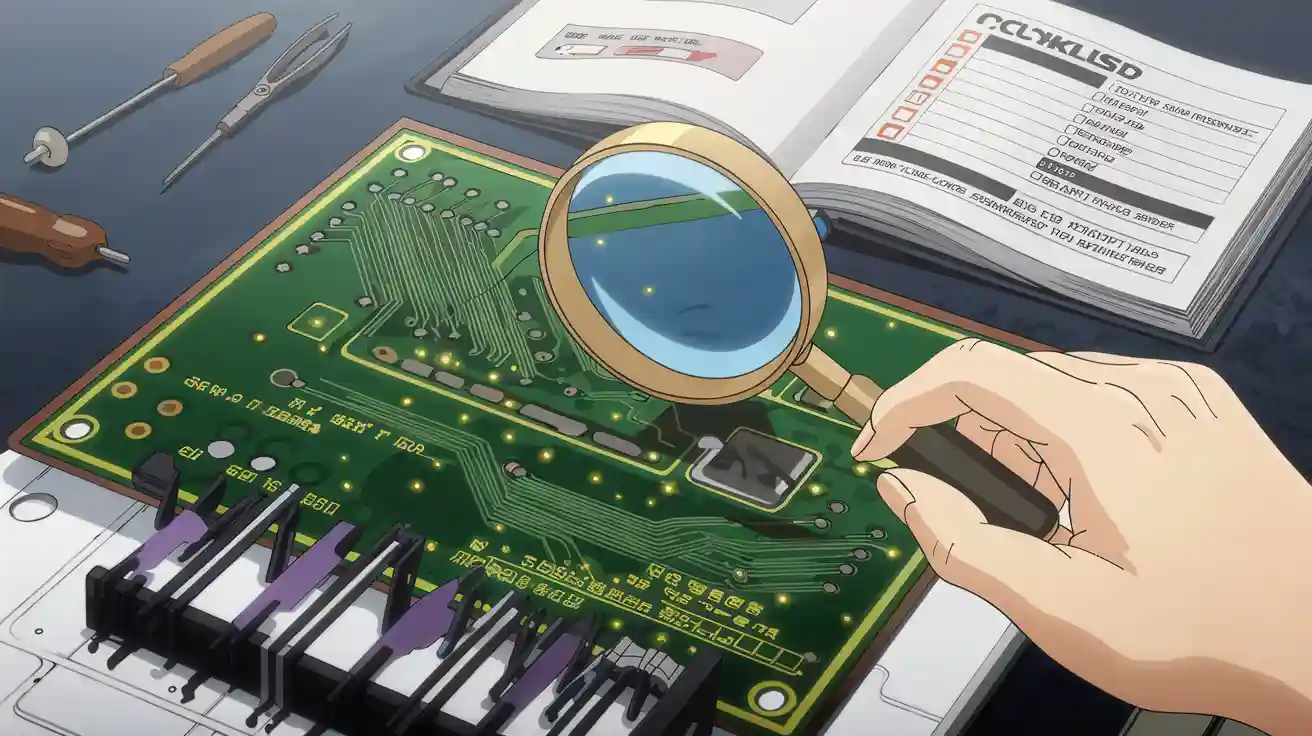
I often see beginners in fpc fabrication struggle with common mistakes that lead to costly setbacks. Some of the most frequent issues I encounter include:
- Failing to clean PCBs thoroughly, which leaves contaminants and causes poor plating adhesion.
- Using the wrong degreasing agents or skipping rinsing steps, resulting in uneven metal deposition.
- Incorrect etching, either over-etching or under-etching, which affects plating quality.
- Mismanaging process fluids, such as using expired or contaminated solutions.
- Rushing or skipping activation and rinsing steps, which creates non-uniform plating and cross-contamination.
Consistent cleaning alone can reduce plating defects by up to 25%. Replacing process fluids after every 500 boards can cut contamination issues by 40%. I always recommend clear planning and careful attention to each step to avoid these pitfalls.
Key Takeaways
- Set clear project goals and keep an accurate parts list to avoid delays and mistakes.
- Choose the right materials and suppliers with quality certifications to ensure reliability.
- Plan component placement and routing carefully to improve performance and reduce errors.
- Test early and often to catch problems before they become costly.
- Keep good documentation and work closely with your team to prevent confusion and improve results.
Project Requirements
Defining Objectives
When I start any fpc fabrication project, I always set clear objectives first. I ask myself what the final product must achieve and what functions it should support. This step helps me avoid confusion later. I write down every requirement, such as size, flexibility, and electrical performance. I also consider the environment where the FPC will operate. For example, if the board needs to bend often, I choose materials that can handle repeated flexing.
Tip: I recommend making a checklist of all project goals before moving to the next step. This habit keeps the project on track and reduces the risk of missing important details.
BOM Accuracy
A precise and up-to-date bill of materials (BOM) is essential for smooth production. I always double-check my BOM before sending it to suppliers. I list every component, including part numbers, quantities, and specifications. Missing or incorrect items can cause delays and extra costs. I have seen projects stall because a single resistor was left off the list.
To avoid these issues, I update the BOM after every design change. I also communicate with my suppliers to confirm that all parts are available. This step helps prevent last-minute surprises during manufacturing, SMT assembly, or transportation.
My BOM checklist includes:
- Component names and values
- Manufacturer part numbers
- Quantity needed
- Special instructions (if any)
By focusing on clear objectives and BOM accuracy, I set a strong foundation for successful fpc fabrication. These steps help me avoid costly mistakes and keep the project moving forward.
Material Selection
Substrate Choice
When I begin a new project, I always pay close attention to the substrate material. The right substrate forms the backbone of a reliable flexible circuit. I often choose polyimide film because it offers excellent flexibility, heat resistance, and durability. This material works well in demanding fields like aerospace and medical devices. Sometimes, I consider polyester (PET) film for simpler applications, but it cannot handle high temperatures as well as polyimide.
Selecting the right substrate means balancing several factors:
- Flexibility for repeated bending
- Resistance to high temperatures
- Protection against chemicals and moisture
- Mechanical strength for handling and assembly
Tip: I always check if the substrate is adhesiveless. Adhesiveless substrates increase flexibility and reduce thickness, which helps prevent delamination and improves performance in harsh environments.
Material Properties
I have learned that every material in a flexible circuit affects its performance and reliability. Here are some key properties I always review:
- Copper Foil Type: Rolled-annealed (RA) copper works best for circuits that bend often. Its grain structure allows it to flex without cracking. Electro-deposited (ED) copper fits static designs.
- Protective Layers: I use coverlay films and solder masks to shield circuits from mechanical and environmental damage. These layers extend the life of the product.
- Stiffeners: When I need extra support at soldering or connector points, I add stiffeners. They provide local rigidity without making the whole board stiff.
- Testing Standards: I follow standards like MIL-PRF-61002 to ensure materials can handle thermal cycling, mechanical stress, moisture, and chemicals.
Note: Choosing the wrong materials can lead to poor flexibility, weak electrical connections, or even early failure. I always match material properties to the needs of the application.
Supplier Selection
Quality Certifications
When I choose a supplier, I always check their quality certifications first. These certifications show that the supplier follows strict standards and can deliver reliable products. I look for the following:
- ISO 9001: This certification guarantees that the supplier has a strong quality management system. It helps reduce defects and ensures consistent manufacturing. I have seen fewer project delays and less rework when working with ISO 9001-certified suppliers.
- IATF 16949: For automotive projects, I need this certification. It covers special requirements for car electronics and helps prevent costly errors.
- UL and RoHS: These certifications confirm that the supplier meets safety and environmental rules. They protect both the end user and the environment.
- IPC-A-610: This standard proves that the supplier meets strict electronics manufacturing guidelines. It is important for high-reliability applications.
Tip: Suppliers with these certifications often provide better documentation, traceability, and technical support. I trust them more because they show a real commitment to quality and safety.
Studies show that certified companies win more contracts and improve efficiency. I always ask for proof of certification before starting any project.
Reliability
Reliability matters just as much as certifications. I evaluate suppliers by looking at their process controls, testing abilities, and communication skills. Here is my checklist:
- The supplier should have documented quality management systems and clear process charts.
- Advanced testing, such as AOI (Automated Optical Inspection) and impedance testing, is a must.
- I check if they use high-quality materials like polyimide, which offers thermal stability and moisture resistance.
- Good suppliers run environmental durability tests, such as humidity and salt spray, to make sure the product lasts.
- I value open communication and long-term support. Reliable suppliers answer questions quickly and help solve problems.
- I avoid suppliers who lack certifications, have weak testing, or communicate poorly.
Note: Choosing the right supplier protects my project from defects like uneven coatings or soldering issues. It also helps me avoid delays and extra costs during manufacturing, SMT assembly, and transportation.
By focusing on certifications and reliability, I build strong partnerships and ensure my projects succeed from design to delivery.
FPC Fabrication Design
Component Placement
When I design a flexible printed circuit, I always start by planning the placement of each component. Good placement helps me avoid manufacturing errors and improves the reliability of the final product. Over the years, I have developed a checklist that guides my decisions:
- I group components by their function. For example, I keep analog parts away from digital ones and separate power supply sections. This reduces interference and makes signal flow smoother.
- I pay attention to thermal management. I place heat-generating parts far from temperature-sensitive components. Sometimes, I use thermal vias or small heat sinks to help remove heat.
- I minimize electromagnetic interference (EMI) by keeping a solid ground plane and separating high-speed from low-speed signals. I also route power traces away from sensitive areas.
- For vibration resistance, I secure heavy components near mounting points. I use symmetrical layouts to balance stress and sometimes reinforce critical parts with adhesives.
- I apply component derating. This means I use parts below their maximum ratings for voltage, current, and temperature. It helps extend the lifespan of the circuit.
- I align components in the same direction. This makes automated assembly faster and reduces placement mistakes.
- I make sure there is enough space for soldering and testing. I avoid placing parts where they block access to test points.
Tip: Careful component placement at the start of fpc fabrication saves time and money later. It also makes the assembly process smoother and more reliable.
Routing & Layout
After placing the components, I focus on routing and layout. Proper routing is critical for signal integrity and overall performance. I have seen many issues arise from poor routing, especially in high-speed designs.
- I avoid placing too many vias, especially in critical signal paths. Each via can add noise and delay. I keep vias short and only use them when necessary.
- I place vias close to component pins. This reduces trace length and helps maintain signal quality.
- I keep enough space between vias and sensitive traces. I follow the rule of at least three times the via diameter for spacing. This reduces crosstalk and interference.
- I use thermal relief patterns on vias. These patterns help manage heat and reduce thermal stress during soldering.
- I always follow the manufacturer's guidelines for via size and placement. This prevents plating failures and broken connections.
- I plan the layout to avoid long or winding traces. Short, direct routes help maintain signal strength and reduce the risk of signal reflections.
Note: Poor routing and layout can lead to signal reflections, crosstalk, and even manufacturing defects. By following these best practices, I improve the reliability and performance of every fpc fabrication project.
Impedance Control
Impedance control is a key factor in advanced flexible circuit designs, especially for high-frequency applications. I always pay close attention to impedance matching to prevent signal reflections and losses. The surface finish I choose, such as ENIG or Immersion Silver, can affect the dielectric constant and trace resistance, which in turn changes the impedance.
I simulate impedance values during the design phase, usually aiming for 50 ohms in RF circuits. I adjust trace widths and spacing to meet these targets. For designs operating above 1 GHz, I request impedance testing reports from the manufacturer.
- I maintain tight impedance tolerances, usually within ±5%. This level of control can reduce signal reflection by up to 40%.
- Precise impedance control lowers signal attenuation by 25% in 5G modules and enables higher data rates.
- It also cuts bit error rates by 60% in millimeter wave applications and improves EMI shielding, which is important for automotive radar systems.
Tip: Customizable layouts and strict impedance control are essential for advanced fpc fabrication. They help me achieve better performance and reliability, especially in demanding environments.
Manufacturing Constraints
Tolerances
I always pay close attention to tolerances during the manufacturing process. Tolerances define the acceptable range for dimensions like trace width, spacing, and hole size. If I set tolerances too tight, I increase production costs and risk delays. If I set them too loose, I may face electrical failures or assembly issues. I work closely with my supplier to match tolerances to the capabilities of their equipment. For example, I specify minimum trace widths and spacing that the factory can reliably produce. I also check that hole diameters fit the components I plan to use.
Tip: I always review the manufacturer’s capability chart before finalizing my design. This step helps me avoid costly redesigns and ensures a smooth transition from design to production.
Method Selection
Choosing the right manufacturing method has a big impact on both cost and quality. I compare the main options before making a decision. For complex, multilayer circuits, I often select the etched FPC process. This method uses photolithography and chemical etching, which allows for fine traces and high reliability. However, it involves many steps and costs more, especially for prototypes. For simple, single-layer circuits, I sometimes choose Flexible Die-Cutting (FDC). This method uses mechanical cutting, which is faster and more environmentally friendly. It works well for basic designs and helps reduce costs.
Here is a quick comparison I use when deciding:
| Aspect | Etched FPC | Flexible Die-Cutting (FDC) |
|---|---|---|
| Circuit Layers | 1 to 8 (multilayer) | Single-layer only |
| Circuit Complexity | Very fine, complex circuits | Simple circuits |
| Manufacturing Cost | Higher, but cost-effective for large runs | Lower for both prototypes and mass production |
| Quality and Reliability | High, proven in critical applications | Still being verified in the market |
| Environmental Impact | Uses chemicals | No hazardous waste |
I always match the method to my project’s needs. For automotive or medical devices, I rely on etched FPC for its reliability. For cost-sensitive or eco-friendly projects, I consider FDC. By making the right choice, I avoid unnecessary expenses and ensure the final product meets all requirements.
Testing & QC
Early Testing
I always start with early testing as soon as I finish the initial design. This step helps me catch problems before they become expensive mistakes. I use prototyping to create small batches and test them in real-world conditions. This process lets me see if the design works as expected and if the materials hold up during use.
- I optimize my PCB design for flying probe testing. This approach reduces testing time by up to 25% and helps me spot errors quickly.
- I place test points where they are easy to reach. This choice lowers the chance of false results and makes troubleshooting faster.
- I work closely with the testing team from the start. Early collaboration helps us find design or process errors before production begins.
- I use advanced design-for-manufacturability tools. These tools catch issues early and save me from costly redesigns.
- I rely on rapid prototyping. Quick iterations let me adjust the design and meet client needs without wasting time or money.
Tip: Prototyping can reduce common issues by 78%. Outsourcing this step to specialists lets me focus on innovation while they handle the risk of errors.
Quality Checks
After early testing, I move on to strict quality checks. I use several methods to make sure every board meets high standards before shipment.
- I use In-Circuit Testing (ICT) to find faults like short circuits, open connections, or wrong component values right after assembly. This step prevents defective boards from moving forward.
- I measure each component’s resistance, capacitance, and voltage. Tight tolerances ensure the board works reliably.
- I catch defects early to avoid expensive repairs and protect my reputation.
Here is a table of the most effective quality check procedures I follow:
| Quality Check Procedure / Practice | Description |
|---|---|
| Design for Testability (DFT) | I add test points and connectors to make testing easier. |
| AOI and ICT | Automated checks reduce manual errors and improve defect detection. |
| Iterative Testing | I test at every stage: prototype, pre-production, and post-assembly. |
| Environmental Testing | I simulate real-world use to find hidden defects. |
| Compliance with Standards | I follow IPC-A-600, IPC-A-610, and AEC-Q100 for quality. |
| Documentation and Collaboration | I keep detailed records and work closely with my team. |
Note: Careful testing and quality checks help me deliver reliable products and avoid costly mistakes.
Communication
Documentation
I always keep detailed documentation for every project. Good documentation helps me avoid confusion and mistakes. I write down every design change, material choice, and process step. I include clear drawings, specifications, and assembly instructions. When I update a design, I make sure the documentation matches the latest version. This habit prevents errors during manufacturing and assembly.
I use a simple table to organize my documents:
| Document Type | Purpose | Who Uses It |
|---|---|---|
| Design Files | Show circuit layout and specs | Designers, Engineers |
| BOM | Lists all parts and quantities | Purchasers, Suppliers |
| Assembly Instructions | Guide for building the board | Technicians |
| Test Procedures | Steps for quality checks | QC Team |
Tip: I always store my documents in a shared folder. This way, everyone on the team can find the latest information quickly.
Collaboration
I believe strong teamwork leads to better results. I work closely with both design and manufacturing teams from the start. We meet often to discuss design choices, material options, and production limits. This teamwork helps us spot problems early and find solutions together.
Here are some ways collaboration improves outcomes:
- We make sure design specs match what the factory can build, especially with special materials.
- We solve challenges like material sensitivity to moisture or heat, design complexity, and cost.
- We prevent issues such as delamination, cracking, and signal problems in complex designs.
- We achieve higher quality, reliability, and performance in the final product.
Note: When everyone shares ideas and feedback, we avoid costly mistakes and deliver better boards to our customers.
Training & Readiness
Formation Training
I always start by making sure my team understands every step of the process. Training forms the backbone of a successful project. I organize hands-on sessions where new team members learn how to handle materials, operate machines, and follow safety rules. I use real-life examples to show what can go wrong if someone skips a step or uses the wrong tool. Mistakes in handling or assembly can lead to broken circuits or wasted materials.
I also create simple guides and checklists. These help everyone remember the correct order of tasks. I encourage my team to ask questions and share their experiences. When someone finds a better way to do something, I update our training materials. This approach keeps our skills sharp and reduces costly errors.
Tip: I recommend regular refresher courses. Even experienced workers can forget small details over time.
Packaging
Proper packaging protects the finished boards during shipping and storage. I never overlook this step. I choose packaging based on the sensitivity of the product. For boards with delicate components, I use anti-static bags and foam inserts. I label each package with handling instructions and destination details.
Here is a table I use to decide on packaging materials:
| Board Type | Packaging Material | Special Instructions |
|---|---|---|
| Standard | Bubble wrap, carton | Keep dry |
| Sensitive/ESD | Anti-static bag, foam | Avoid static discharge |
| Heavy/Stacked | Reinforced box, foam | Handle with care |
I always check that the packaging matches the shipping method. For long-distance transport, I add extra padding. I also track each shipment to prevent loss or damage.
Note: Good packaging saves money by preventing returns and repairs. It also keeps customers happy.
FPC Fabrication Checklist
I always rely on a detailed checklist to keep my fpc fabrication projects on track and minimize errors. Here is the step-by-step process I follow before sending any design to production:
- I start with a thorough Design for Manufacturability (DFM) analysis. This helps me spot potential issues early and avoid costly changes later.
- I use barcode systems to track all materials, including core, prepreg, and copper foil batches. Complete traceability prevents mix-ups and supports quality control.
- I check for stackup symmetry and balance. Mirroring layer count, copper distribution, and dielectric thickness helps prevent bow and twist in the finished board.
- I align the grain direction of all cores and prepregs. This step reduces the risk of shrinkage and warpage during processing.
- I match resin content to copper density, especially on inner layers with heavy copper. This prevents resin starvation and delamination.
- I add copper thieving to sparse layers opposite dense ones. Balanced copper distribution improves lamination uniformity.
- I manage via aspect ratios carefully. I keep hole diameters at or above 0.2 mm for 1.6 mm boards to ensure reliable plating.
- I follow best practices for microvias and via-in-pad designs. Filling and capping vias improves solderability and board strength.
- I provide sufficient annular rings and add teardrops on fine-pitch or high-stress pads. These features enhance mechanical strength and reliability.
- I perform automated optical inspection (AOI) after etching. AOI helps me catch defects like opens, shorts, or incorrect trace widths.
- I use automated X-ray inspection (AXI) after lamination. AXI checks layer-to-layer registration without damaging the board.
- I conduct 100% electrical testing, such as flying probe or bed-of-nails, to verify continuity and isolation across the netlist.
- I control the lamination cycle precisely. A controlled heating ramp rate during gelation ensures consistent quality and yield.
Tip: I keep this checklist visible in my workspace. It reminds me to double-check every step and helps me deliver reliable results in every fpc fabrication project.
I have learned that awareness and proactive steps make a real difference in fpc fabrication. Early detection of material changes and regular monitoring help prevent failures and improve reliability. I always recommend these key actions for beginners:
- Optimize design parameters for clean depaneling.
- Use high-quality tools and materials.
- Protect components and verify fiducial marks.
- Calibrate equipment and follow design guidelines.
- Collaborate with manufacturers and document every detail.
By following these tips and using my checklist, you can approach your first project with confidence and avoid costly mistakes.
.png)
.png)
.png)
.png)

.png)

