


 2025-11-18
 BEST
BEST
You face unique challenges with 32 layer rigid flex pcb design. These rigid flex pcb projects demand strict adherence to design guidelines and industry standards. Advanced rigid-flex pcb technology requires you to consider every detail, from the number of layers and minimum track spacing of 0.075 mm to fold angles and IPC requirements. Design requirements for rigid-flex circuit boards differ greatly from standard flexible circuit boards. Proper pcb design hinges on understanding the specific requirements, layers, and design considerations for rigid-flex pcbs.
Key Takeaways
- Understand the unique features of rigid-flex PCBs. They combine rigid and flexible technologies, allowing for complex designs and reduced connectors.
- Plan your stack-up carefully. Separate signal, power, and ground layers to enhance performance and prevent interference.
- Select appropriate materials. Use polyimide for general applications and consider Liquid Crystal Polymer (LCP) for tight bends and high-frequency needs.
- Follow strict design guidelines. Avoid placing vias in flex areas and maintain proper spacing to ensure reliability and prevent damage.
- Document your design process thoroughly. Keep records of changes and material specifications to support quality control and compliance.
32 Layer Rigid Flex PCB Design Guidelines
Unique Features of Rigid-Flex PCB
You encounter a unique set of challenges when working with 32 layer rigid flex pcb design. These boards combine the best aspects of both rigid and flexible technologies. You gain the ability to create complex three-dimensional assemblies that traditional rigid or flexible PCBs cannot achieve. This hybrid structure allows you to reduce the number of connectors and cables, which improves reliability and saves valuable space.
The table below highlights the main differences between rigid-flex, rigid, and flexible PCBs:
| Characteristic Type | Rigid-Flex PCBs | Traditional Rigid PCBs | Traditional Flexible PCBs |
|---|---|---|---|
| Structural Features | Combination of flexible and rigid materials | Rigid materials only | Flexible materials only |
| Functional Features | Reduces need for connectors, meets multiple functions | Limited to specific functions | Limited to specific functions |
| Manufacturing Complexity | More complex design and manufacturing processes | Simpler processes | Simpler processes |
You see that rigid-flex circuit boards offer a unique combination of flexibility and strength. You can route signals through multiple planes and across moving sections. This capability supports advanced applications in aerospace, medical, and high-end consumer electronics. You must understand these structural and functional differences to apply the right design guidelines for your project.
Advanced Design Methodology
You must approach 32 layer rigid-flex pcb design with a clear strategy. The complexity increases as you add more layers and integrate both rigid and flexible sections. You need to manage signal integrity, mechanical stress, and manufacturability at every stage.
You should use advanced PCB design tools, such as Altium Designer, which supports up to 32 signal layers. This software allows you to visualise the stack-up, manage layer transitions, and check for design rule violations. You can set up constraints for minimum track width, spacing, and pad sizes, which are essential for high-density interconnects.
Tip: Always define your stack-up and layer arrangement early in the design process. This step helps you avoid costly changes later.
You must follow strict design guidelines to ensure reliability. You need to consider the requirements for both rigid and flexible areas. For example, you should avoid placing vias in bend areas and maintain proper spacing between traces. You must also account for the mechanical properties of the materials, such as bend radius and fold angles, to prevent damage during assembly and operation.
You should document every aspect of your pcb design, from material selection to layer configuration. This documentation ensures that your design meets industry standards and passes manufacturing checks. You can improve your workflow by collaborating closely with your manufacturer and reviewing their feedback on your design.
You face a demanding task when designing rigid-flex pcb assemblies with so many layers. You must balance electrical performance, mechanical durability, and manufacturability. By following proven guidelines and using the right tools, you can achieve a robust and reliable product that meets all requirements.
Stack-Up & Material Selection

Rigid-Flex PCB Stack-Up Strategies
You must plan your stack-up carefully when working with 32 layer rigid flex pcb design. The arrangement of rigid and flexible layers affects both electrical performance and mechanical durability. You should separate signal, power, and ground layers to reduce interference. Place flexible layers in areas that require bending or folding. Use a symmetrical stack-up to balance stress and prevent warping.
Note: For high-density pcb design, maintain a minimum track width and spacing of 0.075 mm. This guideline helps you avoid shorts and ensures reliable signal transmission.
You should define pad and hole sizes early in your design. For rigid-flex circuit boards, use a minimum pad diameter of 0.20 mm and a minimum hole size of 0.15 mm. These requirements support manufacturability and long-term reliability.
Material Choices & LCP Considerations
You need to select materials that meet your design guidelines and application requirements. Polyimide remains the standard for most rigid flex pcb projects. For advanced designs, consider Liquid Crystal Polymer (LCP). LCP offers excellent flexibility and low moisture absorption. You can achieve tighter fold angles, typically between 1 and 3 degrees per layer, which is ideal for compact assemblies.
| Material Type | Key Properties | Typical Use Case |
|---|---|---|
| Polyimide | High thermal stability | General rigid-flex pcb |
| LCP | Superior flexibility, low Dk | High-frequency, tight bends |
You should match your material choice to the electrical and mechanical requirements of your pcb design.
Adhesive, Prepreg, and Layer Arrangement
You must use high-quality adhesives and prepregs to bond layers securely. Select adhesives that withstand repeated flexing and thermal cycles. Arrange prepreg layers to reinforce both rigid and flexible sections. You should avoid placing adhesives directly in flex zones, as this can cause delamination.
- Place prepreg between copper layers for insulation.
- Use adhesive only where mechanical strength is needed.
- Stagger layer arrangement to distribute stress evenly.
You improve reliability and manufacturability by following these guidelines. Careful stack-up and material selection ensure your rigid-flex pcb meets all design and performance requirements.
Mechanical & Electrical Design
Signal Integrity & Crosstalk
You must pay close attention to signal integrity when working with 32 layer rigid flex pcb design. High-speed signals can suffer from crosstalk if you do not separate them properly. Place ground planes between signal layers to reduce interference. Keep traces short and direct. Avoid running parallel traces for long distances. You should also use controlled impedance routing for critical signals. IPC-2223 and IPC-6013 offer clear layout guidelines for managing these issues in rigid-flex circuit boards. These standards help you maintain reliable performance across all layers.
Thermal Management
Effective thermal management is essential for high-power rigid flex pcb assemblies. You can use several techniques to control heat:
- Place thermal vias to connect layers and improve heat dissipation.
- Attach heat sinks to absorb and spread heat from key components.
- Position components to allow good airflow and prevent hotspots.
- Apply thermal pads or paste to enhance heat transfer between components and heat sinks.
- Use thermal analysis tools to predict heat flow and optimise your design.
You should always consider these methods during pcb design. Good thermal management extends the life of your assembly and prevents failures.
Mechanical Stress & Flexure
Mechanical stress can damage your rigid-flex pcb if you do not follow proper design guidelines. Always use straight edges and avoid right angles in flex areas. Rounded corners reduce stress and prevent cracking. Maintain a consistent bend radius that matches your material requirements. IPC-2223 and IPC-6013 provide detailed recommendations for flexure and mechanical layout. You should never place vias or pads in areas that bend. This practice helps you avoid fatigue and delamination. Careful planning ensures your design meets both electrical and mechanical requirements.
Tip: Review your pcb design with your manufacturer to confirm that all guidelines and requirements are met before production.
Bend Radius & Flex Area Guidelines
Calculating Bend Radius
You must calculate the bend radius with precision in 32 layer rigid flex pcb design. The bend radius determines how tightly you can fold or flex the board without causing damage. For most rigid flex pcb applications, you should use a minimum bend radius of 10 times the total thickness of the flexible section. This ratio helps prevent cracking and ensures long-term reliability. When you use advanced materials such as LCP, you can achieve tighter fold angles—typically between 1 and 3 degrees per layer—while still meeting design guidelines. Always check the manufacturer’s recommendations for specific requirements based on your chosen materials and stack-up.
Tip: A larger bend radius increases durability and reduces the risk of delamination in rigid-flex circuit boards.
Routing in Flex Areas
Effective routing in flex areas is essential for maintaining signal integrity and mechanical strength. You should avoid placing vias in flex zones, as this prevents stress and potential damage during bending. Microvias work well in high-density designs, but only use them outside the flex regions. To prevent signal degradation, you need to manage impedance carefully, use shielding where possible, and select appropriate trace widths and spacing.
- Keep traces perpendicular to the bend axis.
- Stagger traces between layers to distribute stress.
- Maintain consistent trace width throughout the flex area.
You should involve your manufacturing partner early in the pcb design process. Conduct stack-up reviews to control impedance and follow trace width and spacing recommendations. These steps help you meet the strict requirements of high-layer rigid-flex pcb assemblies.
Preventing Delamination
Delamination poses a significant risk in rigid-flex pcb assemblies, especially when you do not follow proper guidelines. You should avoid sharp corners and right angles in flex areas. Rounded corners distribute stress more evenly and reduce the chance of layer separation. Use high-quality adhesives and prepregs that withstand repeated flexing. Place adhesives only where mechanical strength is needed, not in the main flex zones.
Note: Careful material selection and stack-up planning are your best defences against delamination and early failure.
By following these design guidelines, you ensure your pcb design meets both mechanical and electrical requirements. Proper planning and collaboration with your manufacturer will help you achieve a robust and reliable rigid-flex pcb, even with many layers.
Via & Pad Design in High Layer PCBs

Via Types & Placement
You must select the right via types and placement strategies for 32 layer rigid flex pcb design. Blind, buried, and microvias help you connect multiple layers without increasing board thickness. Place vias outside flex zones to avoid mechanical stress. Use staggered via patterns to distribute current evenly and reduce the risk of hot spots. Always follow design guidelines to ensure reliable connections between rigid and flexible sections.
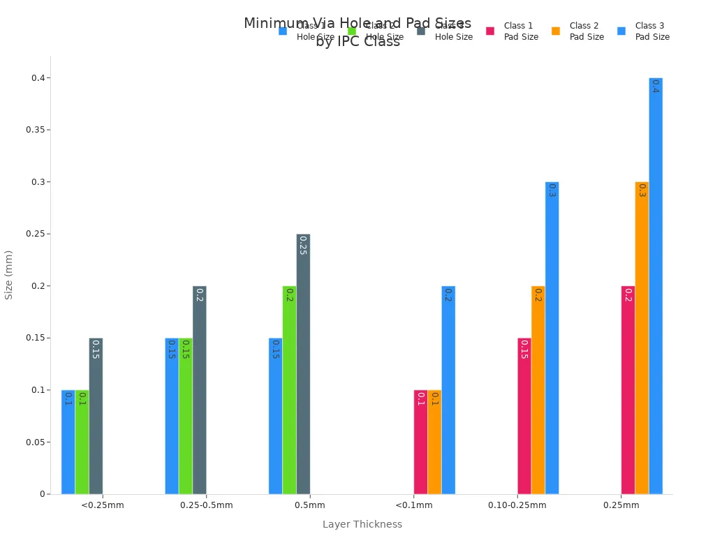
The minimum hole size and pad requirements depend on the layer thickness and IPC class. The table below shows the recommended values:
| Layer Thickness | Class 1 | Class 2 | Class 3 |
|---|---|---|---|
| <0.25mm | 0.10mm | 0.10mm | 0.15mm |
| 0.25-0.5mm | 0.15mm | 0.15mm | 0.20mm |
| 0.5mm | 0.15mm | 0.20mm | 0.25mm |
You can also refer to the following chart for a visual comparison:
Pad Stack Reliability
You need to design pad stacks that withstand repeated thermal and mechanical cycles. Use teardrop-shaped pads to reduce stress at the junctions. Reinforce pads in high-current areas with additional copper. Select pad sizes that match the via hole and meet IPC requirements. This approach prevents pad lifting and ensures long-term reliability for rigid-flex circuit boards.
Tip: Always check your pad stack design with your manufacturer before finalising your pcb design.
Avoiding Via Fatigue
You must prevent via fatigue in high-layer rigid flex pcb assemblies. Avoid placing vias in areas that bend or flex. Use annular rings that meet IPC standards to strengthen the via structure. Distribute vias evenly across layers to minimise localised stress. Regularly review your design to ensure all guidelines are met and update your pcb design as new requirements emerge.
By following these guidelines, you improve the reliability and performance of your rigid flex pcb. Careful via and pad design ensures your assembly meets all electrical and mechanical requirements.
Compliance & Industry Standards
IPC-2223 & IPC-6013 Overview
You must follow industry standards when you work on 32 layer rigid flex pcb design. IPC-2223 and IPC-6013 set the main design guidelines for rigid-flex circuit boards. IPC-2223 covers the generic requirements for flexible and rigid-flex printed boards. It helps you understand how to arrange layers, select materials, and manage mechanical stress. IPC-6013 focuses on the qualification and performance of rigid-flex pcb assemblies. You use these standards to ensure your pcb design meets quality and reliability targets. By following these guidelines, you reduce the risk of failure and improve the performance of your design.
Documentation & Traceability
You need strong documentation and traceability practices to comply with industry standards. Keeping clear records of design changes, material specifications, and testing results supports quality control. This approach also makes troubleshooting easier if problems arise. You can use version control systems to track design changes and improve teamwork. IPC standards provide guidance on how to document and trace test results. Adhering to these requirements helps you meet best practices for pcb design and manufacturing. Good documentation ensures every layer and material in your rigid flex pcb is accounted for throughout the process.
- Maintain records of all design changes.
- Document material specifications and test results.
- Use version control tools for collaboration.
- Follow IPC guidelines for traceability.
Environmental & Safety Standards
You must consider environmental and safety standards during pcb design. Many regions require you to use materials that meet RoHS and REACH regulations. These rules limit hazardous substances in electronic products. You should also check for UL certification if your rigid-flex pcb will operate in demanding environments. Meeting these requirements protects users and the environment. It also helps your product reach global markets. Always review the latest standards before you finalise your design.
By following these compliance and industry standards, you ensure your rigid flex pcb meets all requirements for quality, safety, and reliability.
Manufacturing & Assembly Guidelines
DFM for Rigid-Flex PCB
You improve manufacturability and assembly by following strict design guidelines for 32 layer rigid flex pcb design. You optimise your pcb design by considering corner radii, hole placement, and thickness consistency. You reduce the risk of tears and improve reliability by keeping the minimum radius of corners at least 1.6 mm. You maintain a minimum distance of 0.5 mm from holes to the board edge. You avoid costly errors by ensuring the distance from the transition edge is not less than 1.9 mm from the inner edge of metalised holes. You keep rigid parts at the same thickness to prevent manufacturing issues and increased costs.
| Design Consideration | Description |
|---|---|
| Minimum Radius of Corners | At least 1.6 mm for reliability and tear resistance |
| Distance from Hole to Board Edge | Minimum 0.5 mm |
| Distance from Transition Edge | Not less than 1.9 mm from inner edge of metalised holes |
| Thickness Consistency | Rigid parts should have the same thickness |
Tip: You should always review your pcb design with your manufacturer to confirm that all requirements are met before production.
Assembly Process
You face several challenges during the assembly of rigid flex pcb. You must select and match materials carefully to prevent delamination or warping. You balance the stack-up thickness and manage impedance control to minimise signal integrity problems. You need strict process controls during lamination to avoid misalignment, wrinkles, and voids. You use advanced drilling and via management techniques to protect flexible materials. You test rigid-flex circuit boards rigorously to ensure durability under bending, thermal cycling, and vibration. You monitor manufacturing yield and cost, as complexity increases the risk of defects.
| Challenge | Description |
|---|---|
| Material Selection and Matching | Compatibility of rigid and flexible materials prevents delamination or warping |
| Layer Stack-Up Design | Balancing thickness and managing impedance control |
| Precise Lamination Process | Strict controls avoid misalignment, wrinkles, and voids |
| Drilling and Via Management | Advanced techniques protect flexible materials |
| Reliability Testing | Rigorous tests ensure durability under stress |
| Manufacturing Yield and Cost | Complexity increases risk of defects and raises production costs |
Common Pitfalls
You avoid common pitfalls by following clear guidelines and maintaining close communication with your manufacturer. You prevent delamination by not placing adhesives in flex zones. You reduce the risk of cracking by using rounded corners instead of sharp angles. You avoid signal loss by keeping traces perpendicular to the bend axis. You ensure all layers meet the requirements for both mechanical and electrical reliability. You document every step of your pcb design process to support traceability and quality control.
Note: Careful planning and strict adherence to design guidelines help you achieve reliable and cost-effective rigid-flex pcb assemblies.
PCB Design for Reliability & Testing
Electrical Testing
You must verify every layer of your 32 layer rigid flex pcb design before deployment. Electrical testing ensures that your assembly meets all requirements for performance and safety. You use several essential protocols to check for faults and guarantee reliability.
- Flying Probe Test: This method checks the electrical performance of your rigid flex pcb. It uses moving probes to test each net for continuity and isolation. You can detect open circuits, shorts, and misalignments quickly.
- Automated Optical Inspection (AOI): You use AOI to scan for missing or misaligned components. This process helps you catch errors early in the production cycle.
- In-Circuit Test (ICT): This test checks the function of individual components and verifies correct placement. You confirm that each part works as intended.
You should always follow strict design guidelines for electrical testing. These steps help you avoid costly failures and ensure your rigid-flex pcb meets industry standards.
Mechanical Reliability
You must design your rigid-flex circuit boards to withstand repeated bending and flexing. Mechanical reliability depends on careful material selection and stack-up planning. You should avoid placing vias or pads in flex areas. Rounded corners and consistent bend radii reduce stress on the layers. You test your pcb design by simulating real-world conditions, such as vibration and thermal cycling. These tests help you identify weak points and improve your design before mass production.
Tip: Collaborate with your manufacturer to review mechanical test results and refine your design for maximum durability.
Long-Term Performance
You want your rigid flex pcb to perform reliably over its entire lifespan. Long-term performance depends on robust pcb design, high-quality materials, and strict adherence to guidelines. You should monitor your assemblies for signs of wear, such as delamination or cracking. Regular inspections and accelerated life testing reveal potential issues before they cause failures. You document all test results and design changes to maintain traceability. By following these requirements, you ensure your rigid-flex pcb delivers consistent performance across all layers and applications.
You must follow strict design guidelines to achieve reliable 32 layer rigid flex pcb design. Industry experts highlight key points: avoid vias in flex bends, maintain drill-to-copper clearances, consider flexibility versus layers, and never use sharp angles in flex routing. Use this checklist for your pcb design:
- Select suitable materials for rigid-flex circuit boards.
- Define bend radius and keep components out of flex zones.
- Optimise trace and via design.
- Incorporate stiffeners and position components wisely.
- Adhere to IPC standards and validate requirements.
Continuous learning and collaboration with manufacturers help you adapt to new technologies and meet all design requirements.
FAQ
What is the recommended minimum track width for 32 layer rigid-flex PCBs?
You should use a minimum track width of 0.075 mm. This guideline helps you maintain signal integrity and prevent shorts. Always check with your manufacturer for specific requirements based on your chosen materials and stack-up.
How do you prevent delamination in flex areas?
You avoid delamination by using rounded corners, selecting high-quality adhesives, and keeping adhesives out of main flex zones. You should follow IPC-2223 recommendations and consult your manufacturer for best practices.
Which IPC standards apply to rigid-flex PCB design?
You must follow IPC-2223 for design and IPC-6013 for qualification and performance. These standards help you meet industry requirements for reliability, documentation, and traceability.
Can you place vias in the flexible sections of the PCB?
You should never place vias in flex areas. Vias in these zones increase the risk of fatigue and failure. Always position vias in rigid sections to ensure long-term reliability.
What materials offer the best performance for tight bends?
You achieve the best results with Liquid Crystal Polymer (LCP). LCP provides superior flexibility and low moisture absorption. You can use it for tight bends and high-frequency applications.
.png)
.png)
.png)
.png)

.png)

