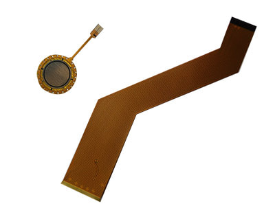
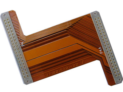
If an end user will specify the copper thickness of a printed circuit, there must be many reasons. For example, current carrying capacity, but copper thickness also directly impacts thermal performance and impedance. All these are vital properties, which have a great influence on the functionality and reliability of a flexible circuit.

At the point, it is important to understand the functional needs driving a copper thickness requirement.
Some of the common functional requirements could be:
1.Minimum thickness in a connector area to assure robust contact.
2.Adequate current carrying capacity directly related to the cross sectional area of the trace.
3.Proper conductivity, a function of cross sectional area and metal type of the trace.
4.Proper impedance in high speed circuits driven by the cross sectional area of the copper, the surrounding dielectric constant, and distance from signal trace to ground plane.
5.Thermal properties directly related to metal type and trace profile.
Copper weight is used in the industry as a “thickness” measurement. Circuit manufacturers commonly purchase copper foil with descriptions of ½ ounce, 1 ounce, 2 ounce and so on. The number is the weight of copper in a square foot of foil. Also, +/- 10% is the industry accepted tolerance for copper foil thickness from the material supplier.

Drawing specifications will frequently define a flexible PCB copper thickness using weight. For example “circuit to be 1 ounce copper”. This can lead to some ambiguity, as copper plating on double sided circuits can easily add an ounce of copper to the surface of a trace. So by specifying thickness in this fashion, it is not clear if this is intended as a finished thickness or an original thickness. Additionally, controlled impedance designs work best when copper plating is restricted to the vias with no copper plated on the surface of the traces. This will minimize trace thickness variability and suggests a specific product category requiring a process known as “Pads Only Plating” or “Button Plating”. For controlled impedance designs, one of these terms should be called out in the drawing notes.
What affects final copper thickness is the variety of manufacturing processes that add or subtract copper thickness. Micro-etching is a common “cleaning” process used to prepare a surface for plating or coating. This process removes a small amount of copper. Likewise copper plating will add thickness. The circuit fabricator will directly measure added (or subtracted) thickness in mils (1 mil =.001”) or microns (25 μm=.001”).
The most accurate method for determining thickness is to do a micro section. This is a destructive test, so it is common to use coupons located in unused areas of the processing panel. These coupons are located and sized to be “representative” of the circuitry copper thickness. Copper thicknesses will vary slightly across a panel depending on current density from electroplating. Current density can be a function of the copper trace pattern so differences among various part numbers will occur. As a general rule, copper plating thickness will tend to be thinner on the outer edges of the panel and thicker toward the center.
In summary, when defining the specific copper thickness for an application it is highly recommended to start with a discussion of the myriad functional requirements. Also, the manufacturer can help recommend copper thicknesses and tolerances as well as the best methods for measurement.
Ebest Circuit (Best Technology) is the professional vendor of flex circuits, from 1 layer to 10 layers, 2 layers rigid-flex circuits to 16 layers rigid-flex circuits, and one-stop service including components purchasing, assembly, IC programming, testing. Choose us, you can always enjoy our best service at a good price.


 2023-03-17
 BEST
BEST

.png)
.png)
.png)
.png)

.png)

