


 2026-10-20

 BEST
A 6-layer HDI rigid-flex PCB combines high-density routing, laser microvias, and flexible interconnections in one compact circuit board. But not every six-layer stackup is straightforward to manufacture. Stacked microvias, thin rigid sections, and fine-pitch components require careful coordination between fabrication and SMT assembly.
BestFPC provides custom 6-layer HDI rigid-flex PCB manufacturing and assembly, including free preliminary DFM review, component sourcing, and quick-turn prototype support. Submit your stackup and fabrication files to check manufacturing feasibility, assembly requirements, and delivery options before placing an order.
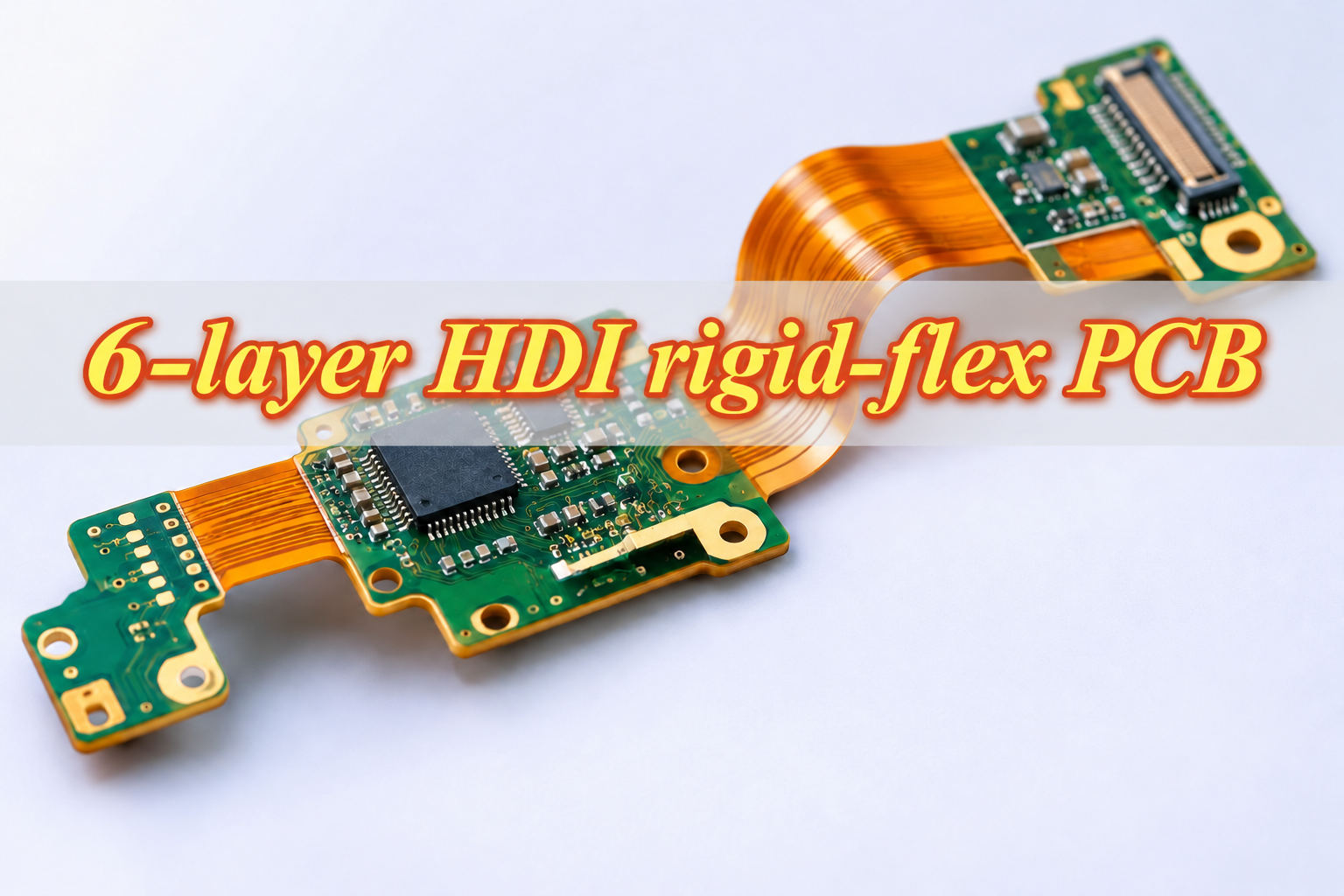
What Is a 6-Layer HDI Rigid-Flex PCB?
A 6-layer HDI rigid-flex PCB combines six conductive layers in its rigid sections with flexible circuits and high-density interconnections. The rigid areas support components and connectors, while the flexible areas connect separate sections without additional cables.
Compared with conventional rigid-flex construction, HDI technology uses laser microvias and finer routing features to accommodate higher component density.
Its main advantages include:
- Higher Routing Density: Supports compact layouts using BGA, WLCSP, and other fine-pitch packages.
- Space and Weight Savings: Replaces selected cables and board-to-board connectors.
- Flexible Integration: Connects multiple rigid sections inside compact or folded enclosures.
- Fewer Connection Points: Reduces the number of separate electrical and mechanical connections.
6-layer HDI rigid-flex PCBs are commonly considered for wearable electronics, medical devices, aerospace modules, industrial sensors, and compact communication equipment.
How Is a 6-Layer HDI Rigid-Flex PCB Stackup Structured?
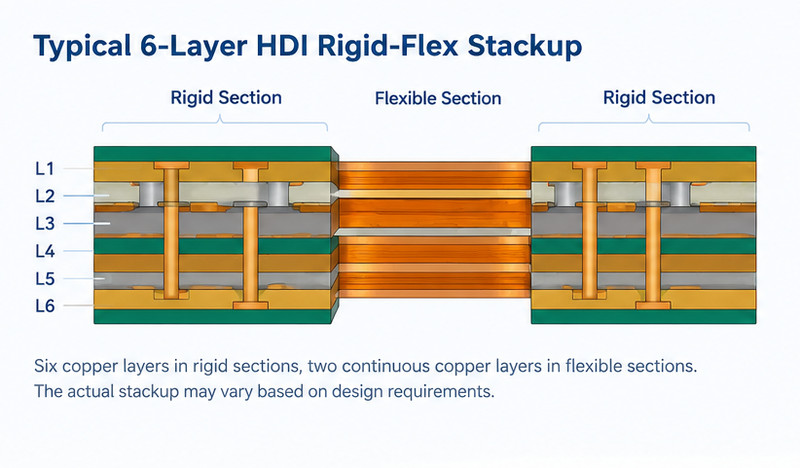
A common six-layer construction uses six copper layers in the rigid sections and two continuous copper layers in the flexible sections. The actual configuration depends on routing density, impedance, finished thickness, and bending requirements.
| Copper Layer | Rigid Section | Flexible Section |
|---|---|---|
| L1 | Outer signal/component layer | Not present |
| L2 | Signal or reference plane | Not present |
| L3 | Signal or reference layer | Flexible copper |
| L4 | Signal or reference layer | Flexible copper |
| L5 | Signal or reference plane | Not present |
| L6 | Outer signal/component layer | Not present |
In this example, L3 and L4 continue through the flexible sections, while L1, L2, L5, and L6 remain within the rigid areas. Other six-layer constructions may use different flexible-layer positions.
An HDI build-up arrangement such as 1+4+1 may also be considered. It describes one outer build-up layer on each side of a four-layer core, not the number of flexible layers. The construction must support both the required HDI interconnections and the rigid-flex material arrangement.
For a manufacturable stackup, confirm copper thickness, dielectric thickness, layer connections, impedance requirements, and rigid-to-flex transitions before releasing the fabrication files.
What Blind, Buried, and Stacked Via Structures Are Used?
Blind microvias, buried vias, and stacked microvias connect selected copper layers without occupying the full board thickness. They provide routing flexibility around fine-pitch components, but each structure has different manufacturing requirements.
| Via Structure | Typical Connection | Manufacturing Requirement |
|---|---|---|
| Blind Microvia | L1–L2 or L5–L6 | Laser drilling and copper plating |
| Buried Via | Internal layers, such as L2–L5 | Inner-layer drilling, plating, and lamination |
| Stacked Microvia | Vertically aligned microvias | Copper filling, registration, and reliable interfaces |
| Staggered Microvia | Offset microvias on adjacent layers | Sufficient routing space and controlled alignment |
Stacked microvias demand tighter process control. Inadequate filling or weak copper interfaces can lead to failures during reflow soldering or thermal cycling, even if the bare board initially passes electrical testing.
A laser microvia may also be formed above a suitable copper-filled buried via, provided the stackup, target-pad geometry, filling process, and lamination sequence support the structure.
For fine-pitch components such as 0.4 mm pitch WLCSP, via-in-pad may be considered to provide routing access beneath the package. Solderable pads containing vias generally require appropriate filling and capping to maintain soldering quality.
What Materials and Thicknesses Are Used in 6-Layer HDI Rigid-Flex PCBs?
6-layer HDI rigid-flex PCBs typically use FR-4-based materials for rigid sections and polyimide laminates for flexible sections. The material combination determines board thickness, bending performance, thermal behavior, and manufacturing compatibility.
- FR-4 Laminate: Provides mechanical support and dimensional stability in rigid sections.
- Polyimide Film: Forms the flexible dielectric structure.
- RA or ED Copper: Selected according to routing density, current requirements, and bending conditions.
- Polyimide Coverlay: Protects flexible conductors while allowing the intended movement.
- Low-Flow or No-Flow Prepreg: Bonds the specified layers while controlling resin movement during lamination.
Rigid and flexible sections require different thickness specifications.
- Rigid Section Thickness: Includes copper layers, dielectric cores, prepreg, and applicable surface coatings. Thin constructions require careful stackup and lamination control.
- Flex Section Thickness: Includes polyimide film, flexible copper, coverlay, and applicable adhesives. Excessive thickness increases bending strain.
- Rigid-to-Flex Transition: Requires controlled material boundaries to avoid localized stress and possible copper damage.
For example, a 0.40 mm finished rigid-section thickness may be requested for a compact electronic enclosure. However, a six-layer construction at this thickness requires a project-specific review of materials, copper weights, and tolerances.
Static bending and repeated dynamic bending are not interchangeable. A flexible section folded once during installation may use a different construction from one subjected to thousands of bending cycles.
How Are 6-Layer HDI Rigid-Flex PCBs Manufactured?
Manufacturing combines multilayer circuit fabrication, buried-via processing, rigid-flex lamination, laser microvia formation, and final inspection. Designs with stacked microvias may require additional build-up and lamination stages.
Step 1: Inner-Layer Fabrication
Rigid and flexible copper layers are patterned according to the approved design. AOI checks circuit features before subsequent processing.
Step 2: Buried Via Processing
Where required, internal layers are drilled and plated before being enclosed by later lamination stages. Registration and copper plating integrity are controlled.
Step 3: Rigid-Flex Lamination
Rigid materials and flexible cores are aligned and laminated. Processing conditions must control resin flow, layer movement, and bonding quality without damaging the flexible sections.
Step 4: Laser Microvia Formation
Laser drilling forms the specified HDI microvias. Target-pad exposure, via geometry, plating, and copper filling are checked. Stacked constructions may require repeated build-up processing.
Step 5: Outer-Layer Processing
Outer copper patterns, solder mask, flexible coverlay, surface finishing, and board profiling are completed according to the fabrication drawings.
Step 6: Inspection and Electrical Testing
Finished bare boards undergo dimensional inspection and electrical testing against the approved manufacturing data.
Step 7: SMT Assembly
For PCBA orders, approved boards proceed through solder paste printing, component placement, soldering, and inspection.
- Fine-Pitch Assembly: BGA, WLCSP, and 0201 packages require suitable stencil design, placement accuracy, and soldering control.
- Double-Sided SMT: Components can be placed on both sides when the layout and assembly sequence permit.
- Assembly Fixtures: Carriers support rigid sections and protect flexible areas during printing, placement, and reflow.
- Inspection: AOI checks accessible joints, while X-ray may be specified for hidden BGA and WLCSP solder connections.
Board support is particularly important when small rigid islands are connected by narrow flexible sections. Inadequate support can cause board movement during placement and soldering.
How Are HDI Microvias and Rigid-Flex Connections Inspected and Tested?
Electrical testing identifies open and short circuits, while structural inspection and reliability testing assess the integrity of HDI interconnections and flexible regions.
| Inspection Method | Main Purpose |
|---|---|
| AOI | Detect circuit-pattern defects, open traces, and shorts |
| Electrical Testing | Verify continuity and isolation |
| Microsection Analysis | Examine via plating, filling, and internal layer structures |
| Dimensional Inspection | Check thickness, hole position, and finished dimensions |
| Thermal Stress Testing | Evaluate interconnections under specified thermal exposure |
| Bend Testing | Assess flexible sections under defined bending conditions |
| X-ray Inspection | Examine hidden solder joints after SMT assembly |
Room-temperature electrical testing alone cannot establish stacked microvia reliability. Weak interfaces may only become apparent during thermal exposure. Critical designs may therefore require representative test coupons and resistance monitoring during qualification.
Special testing and acceptance criteria should be agreed before fabrication, particularly for medical, aerospace, and other high-reliability applications.
What Affects 6-Layer HDI Rigid-Flex PCB Manufacturing and Assembly Costs?
The cost depends on HDI complexity, materials, thickness tolerances, manufacturing quantity, and assembly requirements. Two six-layer boards with similar dimensions may require very different processing.
- HDI Build-Up: Additional lamination cycles increase processing requirements.
- Via Structure: Buried vias, stacked microvias, and copper filling add fabrication operations.
- Material and Thickness: Thin rigid sections, specialized laminates, and tight tolerances affect material selection and production.
- Fine-Line Routing: Narrow traces and spaces require more precise imaging and etching.
- SMT Assembly: Fine-pitch packages, double-sided placement, and special fixtures increase assembly complexity.
- Order Quantity and Testing: Prototype setup, production volume, and specialized inspection affect total costs.
A stacked microvia structure generally requires more processing than a comparable single-level microvia construction. The difference becomes greater when additional filling, lamination, and reliability testing are necessary.
For an accurate quotation, separate PCB fabrication, setup, component sourcing, SMT assembly, and special testing costs.
Why Choose BestFPC for 6-Layer HDI Rigid-Flex PCB Manufacturing & Assembly?
BestFPC provides custom rigid-flex PCB fabrication and SMT assembly through one manufacturing partner, helping customers coordinate complex PCB projects from prototype review through production.
- Free Preliminary DFM Review: Check stackup feasibility, via construction, finished thickness, bend regions, and manufacturing tolerances before fabrication.
- Custom HDI Rigid-Flex Manufacturing: Evaluate multilayer structures, fine-line routing, blind/buried vias, controlled impedance, and customized material requirements.
- In-House PCB Manufacturing & SMT Assembly: Coordinate bare-board fabrication, component sourcing, assembly, and inspection while reducing supplier handoffs.
- Quick-Turn Prototyping: Support engineering prototypes and small-batch orders. Expedited delivery is evaluated against manufacturing complexity and material availability.
- Reliable Quality Control: Provide electrical testing, inspection, and project-specific quality requirements according to the approved manufacturing scope.
- Flexible Component Sourcing: Support turnkey, partial-turnkey, and customer-supplied component arrangements.
BestFPC operates in Shenzhen, China, supporting prototype and production requirements for customers worldwide. For complex six-layer HDI constructions, the exact fabrication capability and delivery schedule are confirmed after reviewing the submitted files.
Case Studies: 6-Layer HDI Rigid-Flex PCB for Wearables Applications
Project Background
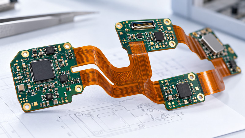
A compact wearable device requires several component-mounting areas inside a small enclosure. Using a 6-layer HDI rigid-flex PCB allows separate rigid sections to connect through flexible circuits without additional board-to-board connectors.
Technical Requirements
- 6 conductive layers in the rigid sections and 2 continuous flexible copper layers.
- Blind microvias for high-density routing around compact components.
- A proposed 0.40 mm rigid-section thickness, subject to stackup feasibility.
- 0.4 mm pitch WLCSP and 0201 components for high-density SMT assembly.
- Controlled bending regions and reliable connections between rigid sections.
Manufacturing and Assembly Approach
The first task is to verify whether the 6-layer stackup and 0.40 mm thickness target can be manufactured with compatible materials and acceptable tolerances.
The review then checks laser microvia geometry, filling requirements, and the placement of vias relative to the flexible regions. Any stacked microvia structure must be evaluated for manufacturing and reliability risks.
For SMT assembly, the small rigid sections require support fixtures during solder paste printing, component placement, and reflow. The proposed inspection plan includes bare-board electrical testing and appropriate inspection of hidden WLCSP solder joints.
Project Results
The review would establish the feasible stackup, via structure, assembly fixtures, and inspection requirements before prototype production.
Actual manufacturing yield, test results, and delivery time must be verified through a completed build. These values cannot be assumed from the proposed design.
What Files Are Required for a 6-Layer HDI Rigid-Flex PCB Quote?
A complete RFQ should include manufacturing files, stackup details, assembly requirements, and separate bare-board and assembled-board quantities.
Gerber or ODB++ Files: Complete PCB fabrication data.
- Drill Files: Mechanical holes, laser microvias, buried vias, and layer connections.
- Stackup and FAB Drawing: Materials, copper thickness, dielectric construction, finished thickness, and tolerances.
- Mechanical Drawing: Rigid/flex boundaries, bend locations, finished dimensions, and stiffener requirements.
- BOM and Pick-and-Place Files: Component specifications and placement data for SMT assembly.
- Order Details: PCB quantity, assembled quantity, delivery destination, and required date.
- Quality Requirements: IPC acceptance class, inspection criteria, and any special qualification.
For designs using stacked microvias over buried vias, include the complete via dimensions, connection layers, counts, and fabrication notes. These details are necessary for an accurate manufacturing assessment.
FAQs About 6-Layer HDI Rigid-Flex PCBs
Q1: Should flexible sections use polyimide coverlay instead of solder mask?
A1: Polyimide coverlay is generally preferred for bending regions because it provides insulation while accommodating flexing. Conventional solder mask is more commonly used on rigid sections.
Q2: How close can copper traces run to the rigid-to-flex transition?
A2: There is no universal clearance for every construction. Trace placement depends on the transition geometry, coverlay boundary, and mechanical strain. The required clearance should be confirmed during DFM review.
Q3: Can plated through-holes be placed in areas that will bend?
A3: Plated holes should generally remain outside bending regions. Hole barrels and surrounding pads can concentrate mechanical stress and increase the risk of cracking.
Q4: Do stacked microvia test coupons need to match the production board?
A4: Yes. Test coupons should represent the critical via geometry, layer connections, and processing conditions of the production board. The required acceptance criteria should be agreed before manufacturing.
Q5: Can a flexible section be twisted as well as bent during installation?
A5: Only if the construction is suitable for the combined movement. Twisting introduces additional mechanical strain, requiring evaluation of the flexible materials, copper routing, and installation geometry.
Q6: Can connectors be mounted close to the rigid-to-flex boundary?
A6: Yes, with adequate support and clearance. Connector insertion forces must not place excessive stress on the transition or adjacent flexible conductors.
Q7: How should finished rigid-flex PCBs be packaged before SMT assembly?
A7: Packaging should protect against mechanical damage, electrostatic discharge, and moisture exposure as applicable. Flexible sections need protection against unintended bending and creasing during handling and transportation.
Q8: Can additional stiffeners be attached without changing the main rigid-flex stackup?
A8: Yes. FR-4 or polyimide stiffeners may reinforce selected areas. Their thickness, attachment method, and clearances must be included in the manufacturing requirements.
Q9: Can a production order be divided into separate SMT assembly batches?
A9: Yes. Assembly quantities can be divided into batches according to the agreed production plan. Component availability, PCB storage conditions, and batch traceability should be considered.
Q10: Can alternative components be used if an approved BOM part becomes unavailable?
A10: Only with customer approval. Substitutes must be checked for electrical specifications, package dimensions, footprint compatibility, and assembly requirements before use.
Conclusion
A reliable 6-layer HDI rigid-flex PCB starts with the right stackup, manufacturable microvia structures, controlled thicknesses, and an assembly process suited to its mechanical design. Confirming these requirements early helps avoid fabrication changes and unexpected production delays.
Ready to manufacture your 6-layer HDI rigid-flex PCB? BestFPC provides free preliminary DFM review, custom PCB fabrication, SMT assembly, and quick-turn prototype support. Send your Gerber files, stackup, FAB drawing, and BOM to sales@bestfpc.com. Our team can review manufacturing feasibility, identify potential fabrication and assembly issues, and prepare a project-specific quotation with a confirmed delivery schedule. Get your project reviewed and move it toward production with BestFPC.


.png)
.png)
.png)
.png)

.png)