


 2023-01-05
 BEST
BESTAs we all know, EMI shielding is used to block the signal. But it must be grounded and then has the block signal function. So how do we connect EMI film to GND? What should we pay attention to in EMI shielding design in flexible circuit boards? Ebest Circuit (Best Technology) would like to share some guidelines about EMI shielding in flexible circuits with you today.
What is EMI shielding?
EMI (Electromagnetic interference) Shielding in electronic devices and equipment is the use of manufacturing techniques and materials to protect signals from being disrupted by external electromagnetic signals as well as preventing generated signals from interfering with surrounding components. Essentially, EMI shielding serves to block these signals from entering or exiting a portion of a part or product.
EMI shielding is created by three components -- the source, path and receiver. The source and receiver are two systems that are responsible for coupling signals from one system to another. In general, the source is an external circuit or phenomenon that creates the interference, which can be naturally occurring (lightning, auroras, cosmic microwave background and solar flares) or artificial (cellular networks, AM/FM radio waves, power transmission lines, measurement and control devices). The receiver, or the victim, is the sensor signal or device in which its output signal is distorted by the disturbance. The path is where signal coupling occurs, which can be through four modes – Conducted EMI, Radiated EMI, Capacitive EMI and Magnetic EMI. The Capacitive EMI and Magnetic EMI can occur at a very close distance.
Importance of EMI Shielding
With the rapid development of advanced technology, electronic devices existing in everywhere we can see and touch. This wide array of electronics has the potential danger to damage and interfering with each other unless they are shielded properly. EMI shielding aims to isolate the energy of a device so that it does not affect what is around it and blocks external energy from attacking.
With a deep understanding of the nature of EMI, it is clear that it can affect its surroundings in various ways. It can affect electronics that are in contact (conducted EMI), in close proximity without contact (capacitive and magnetic EMI), and even over large distances (radiated EMI). Along with the progress of the information age, the increased usage of electronics for data processing and communication creates considerable pollution to the electromagnetic wave spectrum, on top of the other disturbances caused by electrical transmission and distribution systems and natural phenomena such as lightning strikes and solar flares. Below are some effects of EMI.
- Jammed or distorted signals received by communication devices
- Sudden power outages, power fluctuations, and electrical fast transitions (EFT)
- Total electronic circuit failure or damage
- Decreased life and performance of electronic systems
- Electric shock and burns
- Potential ignition source
EMI shielding design
To avoid the signals be damaged or interfered with, EMI shielding can be considered the most cost-effective method of EMC compatibility since it decreases the use of intra-equipment devices to manage undesired signals. Achieving EMC through shielding depends on two factors: the structural or form design and the materials used. A simple EMI shield design is a Faraday cage made of conductive materials such as copper. The EMI shield design depends on the characteristics of the electromagnetic environment within which the equipment must reliably function. Below are some design considerations for constructing an EMI shield.
1. Connect EMI film to GND through a small coverlay opening only from one side for both top and bottom EMI film coating only, it can’t be GND through via. Because the EMI is very thin, it will be easy to break.
2. Coverlay opening area for the pad on copper size should be equal to or more than 0.8mm, the shape of a circle or oval, circle will be better.
3. Discontinuities must be minimized to control leakage of radiated EMI.
4. In case permanent bonding is not possible, ensure that the chosen fastening method exerts enough pressure to maintain contact.
5. Generally, similar metals are bonded to prevent galvanic corrosion.
6. The poorest electrical bond will determine the shielding effectiveness of the enclosure.
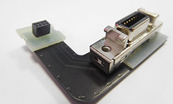
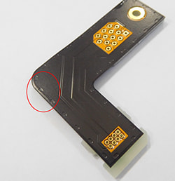
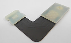
7. If the FPC cable some areas need PI, FR4 or stainless stiffeners, we suggest the EMI far away from the stiffeners 1mm at least to avoid the poor binding EMI shielding fall off. It's okay to use EMI coating under the stiffener if the pins of the connector have been soldered to the FPC and stiffener firmly after assembling as attached pictures.
|
|
|
|
8. For EMI shielding on the top and bottom side we suggest one side close to left 0.5mm, and another side close to the right 0.5mm. Because the EMI shielding will have a 0.3mm stick tolerance, it will be easy to have a stress trace on the EMI shield.
Do you have any questions about EMI shielding? Or does any similar flex PCB need to produce? Please feel free to contact us at sales@bestfpc.com
.png)
.png)
.png)
.png)

.png)

