


 2026-03-02
 BEST
BESTTable of Contents
- What Is the mSAP Process and Why It Matters for Ultra-HDI FPC
- UK Industrial Expectations for Ultra-HDI FPCs Using mSA
- Engineering Factors and Best Practices in mSAP-Based FPC Manufacturin
- Manufacturing Challenges and Solutions with mSAP for Ultra-HDI FPC
- FAQ – mSAP Process for Ultra-HDI FPC Manufacturing
- Why BESTFPC Is the Right Choice for Ultra-HDI mSAP FPC Projects
- Conclusion & Next Steps for UK Design Engineers

What Is the mSAP Process and Why It Matters for Ultra-HDI FPCs
The modified Semi-Additive Process (mSAP) is an advanced PCB fabrication technique that enables ultra-fine line widths, high wiring density, and exceptional feature control — capabilities that traditional subtractive processes (etching) struggle to achieve. Instead of etching away unwanted copper from a thick copper sheet, mSAP adds copper only where circuit patterns are required using additive plating techniques. This allows for greater precision in trace geometry, reduced material waste, and higher interconnect density — features essential for Ultra-HDI Flexible Printed Circuit (FPC) boards.
mSAP Defined vs Traditional PCB Fabrication
In traditional subtractive PCB manufacturing, a full copper sheet is laminated to the substrate and unwanted copper is chemically etched away. This leads to:
- Limitation in how narrow a trace can be reliably etched
- Tapered edges and potential signal distortion
- Wasted material removed during etching
By contrast, mSAP builds up copper directly where needed, achieving fine traces and spaces with near-vertical sidewalls and minimal undercut. The process typically involves:
- Depositing a very thin seed copper layer on the substrate
- Applying photoresist and patterning the circuit image
- Plating copper into the exposed areas to build conductive traces
- Stripping resist and removing the unwanted seed layer
This yields cleaner trace profiles and enables ultra-fine features that are ideal for high-performance applications.
Technical Advantages of mSAP in Ultra-HDI FPC
The use of mSAP unlocks several advantages over traditional methods:
- Ultra-fine traces and spaces: mSAP can achieve line/space patterns down to ≤30 µm, making it suitable for high-density interconnects required by next-generation devices.
- Improved signal integrity: The additive nature reduces sidewall roughness and provides more uniform trace cross-sections, improving high-frequency performance.
- Thinner, lighter circuits: mSAP supports thinner copper layers on ultra-thin substrates (down to ~25 µm total thickness), yielding lighter boards suited to flexible applications.
- Better reliability: Enhanced adhesion and fewer stress points improve the mechanical endurance of Ultra-HDI FPCs under bending, thermal cycling, and vibration.
These benefits make mSAP a core technology for Ultra-HDI Flexible PCBs in advanced electronics and communication systems.
UK Industrial Expectations for Ultra-HDI FPCs Using mSAP
In the UK market, several key sectors are pushing the demand for mSAP-enabled Ultra-HDI FPCs due to their stringent performance and miniaturisation needs.
Telecommunications Infrastructure & 5G/6G
Next-generation telecom systems (5G and emerging 6G prototypes) require boards with tight impedance control and ultra-fine traces to support high-frequency signal routing with minimal losses. Ultra-HDI FPCs manufactured via mSAP ensure compact, high-speed interconnects for base stations, small cell modules, and mmWave hardware, where every micron of trace accuracy influences signal integrity and bandwidth performance.
Industry Insight:
Internal links to pages like Telecommunications PCB Solutions and High-Speed Signal Integrity Design help address UK telecom engineer queries and improve engagement.
Medical Electronics & Wearables
Medical devices — such as portable diagnostic tools, wearable biosensors, and implantable modules — require compact, flexible boards with ultra-fine routing to pack more functionality into small form factors. mSAP-based Ultra-HDI FPCs help designers achieve:
- Higher component density
- Predictable high-frequency performance
- Better mechanical reliability under chronic flex
UK medical engineers increasingly specify Ultra-HDI designs to meet both regulatory and usability goals.
Aerospace & Defence Applications
Aerospace and defence electronics in the UK demand high-performance flexible circuitry capable of enduring extreme thermal, vibration, and environmental stresses. Ultra-HDI boards manufactured via mSAP provide:
- Fine pitch routing for complex sensor arrays
- High thermal reliability
- Compact integration with rigid mounting points
The precision inherent in mSAP supports design specifications for critical avionics systems and rugged defence modules.
Industrial Automation & Sensors
In industrial environments, compact and flexible PCBs enable smarter sensing, robotic joints, and tight-space interconnects. Ultra-HDI FPCs with mSAP precision help:
- Maximise wiring density in control modules
- Maintain signal fidelity in high noise environments
- Integrate sensors and actuators with minimal routing length
UK manufacturers in automation and smart infrastructure increasingly require boards that blend flexibility with HDI performance.
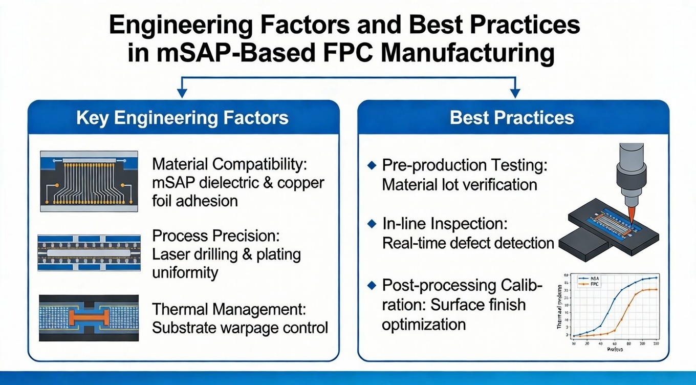
Engineering Factors and Best Practices in mSAP-Based FPC Manufacturing
Achieving consistent high quality in Ultra-HDI Flexible PCB fabrication using mSAP requires careful attention to engineering details across material, process, and validation stages.
Material Selection & High-Density Design
Selecting an appropriate substrate is essential. Flexible boards for Ultra-HDI applications typically use polyimide films due to high thermal stability and mechanical resilience. Substrate roughness needs to be controlled to ensure optimal copper adhesion during additive plating. High-density designs demand uniform dielectric properties to maintain controlled impedance and signal integrity, especially at higher frequencies.
Designers should integrate early simulation and modeling into the HDI stack-up to predict high-frequency performance and identify potential hotspots or impedance mismatch regions before manufacturing.
Precision Trace Control & Fine Pitch Limitations
To harness the advantages of mSAP, manufacturers must tightly control trace dimensions and spacing. Unlike subtractive etching, mSAP builds copper traces directly and enables ultra-fine features, but this demands:
- High-resolution photolithography for pattern definition
- Stable electroless plating chemistry for seed layer deposition
- Consistent electroplating control for thickness uniformity
Industry benchmarks suggest mSAP can produce trace widths and spacings down to 30 µm or below, supporting high wiring densities without compromising reliability.
Inspection, Quality Assurance & Metrology
High-precision manufacturing must be backed by robust QA systems. Advanced inspection tools like 3D automated optical inspection (AOI), X-ray imaging, and in-process metrology help detect defects early. Impedance testing and microsection analysis verify that trace integrity meets design and performance criteria.
Linking to internal pages like PCB Quality Control and Ultra-HDI Design Guidelines will help guide UK engineers to deeper engagement points aligned with GSC interaction data.
Manufacturing Challenges and Solutions with mSAP for Ultra-HDI FPCs
Producing Ultra-HDI flex PCBs with mSAP introduces several manufacturing challenges that top-tier facilities like BESTFPC address with advanced process controls and investment in equipment.
Process Complexity and Equipment Demands
mSAP requires equipment capable of:
- Electroless copper seed layer deposition
- Precise photolithography (sub-10 µm patterning)
- Controlled electroplating with uniform thickness (e.g., Uniplate IP3 systems)
These capabilities ensure tight process control and high yield rates, even for complex multilayer Ultra-HDI structures.
Yield Optimisation and Defect Control
High wiring density increases the risk of shorts, opens, and microimprint defects. Solutions include:
- Closed-loop process monitoring
- In-line inspection and feedback loops
- Controlled lamination and handling to prevent contamination
Proactive defect reduction directly improves manufacturability and reduces scrap rates.
Cost and Throughput Considerations
While mSAP enables premium performance, associated capital and operational costs can be higher than traditional processes. Efficient batch scheduling, standardisation of panel sizes, and automation help mitigate cost pressures while maintaining throughput.
FAQ – mSAP Process for Ultra-HDI FPC Manufacturing
Q1: What does mSAP stand for and what makes it different?
mSAP stands for Modified Semi-Additive Process, which adds copper only where traces are needed, enabling ultra-fine lines and high wiring density beyond traditional etching.
Q2: Can mSAP be used for flexible PCBs?
Yes — mSAP is well-suited for Ultra-HDI Flexible Printed Circuit Boards, providing precise routing, improved adhesion, and fine features.
Q3: Why is mSAP important for high-frequency applications?
By enabling tighter trace control and better impedance uniformity, mSAP supports high-frequency performance critical to telecom, 5G/6G modules, and advanced RF applications.
Why BESTFPC Is the Right Choice for Ultra-HDI mSAP FPC Projects
BESTFPC blends advanced manufacturing expertise with deep understanding of high-density flexible PCB requirements:
- Experienced engineering support for mSAP stack-ups and HDI layouts
- Production systems capable of ultra-fine features with controlled tolerances
- Rigorous QA with in-line metrology and high-precision inspection
- UK-focused guidance on design optimisation, material selection, and reliability considerations
By aligning production with customer specifications and regulatory expectations — including sustainable and high-performance design principles — BESTFPC helps UK engineers accelerate prototype to volume transitions with confidence.
Conclusion & Next Steps for UK Design Engineers
The mSAP process for Ultra-HDI FPCs represents a pivotal advancement in high-precision flexible PCB manufacturing. From ultra-fine trace control and improved signal integrity to compact high-density layouts, mSAP enables next-generation electronics in telecom, medical, aerospace, and industrial sectors.
For UK engineers seeking reliable production partners with advanced mSAP capabilities, BESTFPC combines technical depth, robust production systems, and engineering collaboration — delivering Ultra-HDI Flexible PCBs that meet exacting performance and quality expectations.
.png)
.png)
.png)
.png)

.png)

