


 2025-10-17
 BEST
BEST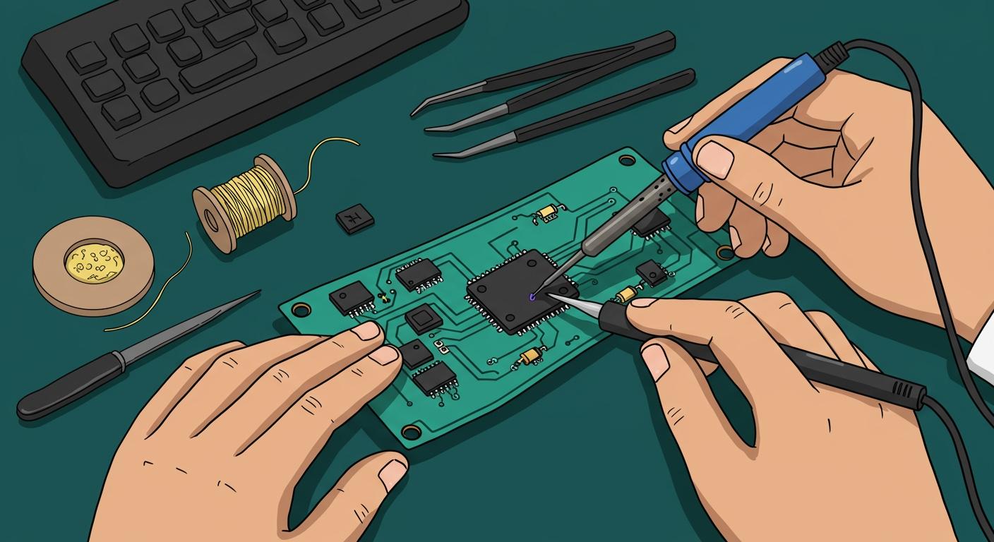
When you work with flexible pcb soldering, you must control heat and minimize stress at every step. Flexible circuits often use materials like polyimide or FR-4, which react differently to heat and moisture compared to rigid boards. For example, standard FR-4 can warp or deform during reflow because of its low glass transition temperature and high coefficient of thermal expansion. See the table below for how common materials impact soldering reliability:
| Material Type | CTE (ppm/°C) X-Y | CTE (ppm/°C) Z | Tg (°C) | Moisture Absorption (%) | Impact on Soldering Reliability |
|---|---|---|---|---|---|
| Standard FR-4 | 14-17 | 70-85 | 130-140 | 0.1-0.2 | Risk of warpage and deformation during reflow due to low Tg and high CTE mismatch. |
| High Tg FR-4 | N/A | N/A | 170-180 | N/A | Better stability during reflow, reducing risk of structural issues. |
| Metal-Core PCBs | N/A | N/A | N/A | N/A | Excellent heat distribution minimizes thermal gradients, reducing warpage risk. |
| Ceramic Materials | N/A | N/A | N/A | N/A | Superior thermal properties but limited by cost and brittleness. |
You need to approach each solder joint with care to prevent mechanical damage and ensure long-term reliability.
Key Takeaways
- Control heat carefully during soldering. Use low-temperature soldering between 260°C and 290°C to prevent damage to flexible circuits.
- Minimize mechanical stress on flexible PCBs. Use stiffeners under components to distribute stress and avoid microcracks.
- Choose the right tools and materials. A temperature-controlled soldering iron and lead-free solder are essential for safe and effective soldering.
- Pre-bake PCBs to remove moisture. This step prevents defects like blistering and ensures better solder joint reliability.
- Inspect solder joints thoroughly. Use visual checks and tools like X-ray inspection to catch defects early and ensure long-lasting connections.
Key Principles For FPC Soldering
Controlled Heat
You must control heat precisely during flexible pcb soldering. Flexible circuits, especially those made from polyimide, can suffer damage if exposed to excessive temperatures. Use low-temperature soldering, ideally between 260°C and 290°C, to protect the substrate and prevent warping. Pre-baking the PCB helps remove moisture and reduces the risk of delamination. The recommended baking times vary depending on the circuit type and layer count:
| Method | Details |
|---|---|
| Baking Time for Single & Double-Sided Circuits | 2 to 3 hours at 105 to 115°C |
| Baking Time for Three-Layer Polyimide Circuits | 3 to 4 hours at 105 to 115°C |
| Baking Time for Four Layers and Above | At least 4 hours at 105 to 115°C |
| Baking Time for Rigid-Flex PCB | 2 hours for up to 1.0 mm thickness; up to 6 hours for 1.8 to 4.0 mm thickness |
| Post-Baking Storage | Store below 50% relative humidity; use vacuum or oven at 35°C with desiccant |
You should avoid overheating, which can cause microcracks and reduce the lifespan of solder joints. Always use a temperature-controlled soldering iron and monitor the process closely.
Minimal Stress
Minimizing mechanical stress is essential for reliable flexible pcb soldering. Mechanical stress during soldering can lead to microcracks, low-cycle fatigue, and eventual electrical failure. Voids in solder joints also increase the risk of crack initiation. Flexible circuits require gentle handling because their unique mechanical properties make them more susceptible to damage.
Tip: Use stiffeners under components to distribute stress evenly. Stiffeners should cover at least half the component area for best results.
Industry standards recommend reducing stress in assemblies, especially where boards bend or experience thermal cycling. Stress can cause trace cracking, component failure, or delamination. You should always wear safety goggles and handle the PCB with care to prevent accidents.
- Mechanical stress from different CTEs can cause microcracks over time.
- Thermal cycling induces stress, affecting solder joint fatigue life.
- Grain structure of solder joints influences stress transfer during temperature changes.
By following these principles, you improve the reliability and longevity of your flexible PCB assemblies.
Tools and Materials For Flexible Circuit Soldering
Choosing the right tools and materials is essential for successful flexible pcb soldering. You need equipment that delivers precise heat, uses the correct solder and flux, and keeps you safe from common risks.
Soldering Iron and Tips
You should select a temperature-controlled soldering iron with a fine tip. This setup gives you better control and helps prevent overheating delicate flex circuits. Two popular models stand out for flexible pcb soldering:
| Soldering Iron Model | Key Features | Price |
|---|---|---|
| X-Tronic Model 3020-XTS | Fast heat-up, ergonomic grip, digital temperature display, sturdy stand | $55 |
| Hakko FX-888DX | Quick heat-up, solid build, digital display, comfortable handle | $121 |
A fine tip allows you to target small pads without spreading heat to nearby traces. Always check that your iron maintains a steady temperature during use.
Solder and Flux Choices
You must choose solder and flux carefully. Lead-free solder is now the industry standard for flexible pcb soldering. It protects your health and meets environmental regulations, but it requires more skill because of its higher melting point and different flow characteristics.
| Advantages of Lead-Free Solder | Disadvantages of Lead-Free Solder |
|---|---|
| Health and safety benefits | Higher melting point can damage components |
| Reduces risk of lead poisoning | Less even and fluid melting |
| Complies with regulations | More likely to fail under stress |
| Preferred for mass production | Wettability issues, needs skill |
For flux, you have several options. Rosin flux works well for strong cleaning, no-clean flux leaves little residue, and water-soluble flux is easy to clean but needs thorough rinsing.
| Type of Flux | Characteristics | Best For |
|---|---|---|
| Rosin Flux | Pine resin-based, various activation levels | Strong cleaning, non-strict residue needs |
| No-Clean Flux | Minimal, non-corrosive residue | High-speed, no-cleaning environments |
| Water-Soluble Flux | Highly active, easy water cleanup | High activity, thorough cleaning allowed |
Safety Equipment
You must protect yourself and your work. Always use safety goggles to shield your eyes from splashes and fumes. Set up a grounded workstation and use anti-static mats and wrist straps to prevent electrostatic discharge (ESD) damage. Thermal shock protection helps avoid delamination or trace damage.
| Safety Equipment | Risk Mitigated |
|---|---|
| Grounded Workstations | Electrostatic Discharge (ESD) damage |
| Anti-static Mats | Electrostatic Discharge (ESD) damage |
| Wrist Straps | Electrostatic Discharge (ESD) damage |
| Thermal Shock Protection | Delamination or trace damage |
Tip: Always check your safety gear before starting flexible pcb soldering. A safe workspace leads to better results and fewer accidents.
Flexible PCB Soldering Steps
Pre-Baking
Pre-baking is a critical first step in flexible pcb soldering. You remove moisture and volatiles from the PCB materials, which prevents outgassing and blistering during soldering. Industry standards, such as IPC-1601, recommend this process to eliminate contaminants. NASA also sets strict outgassing limits for materials used in space, highlighting the importance of this step.
- Pre-baking helps you avoid thermal defects and reduces the risk of dielectric breakdown.
- Moisture trapped in the board can cause blistering and lower the reliability of your solder joints.
- For Pyralux® Flex materials, bake at 250°F (121°C) for 2 to 10 hours, depending on thickness and design.
- You can use lower temperatures (150-175°F or 65-80°C) in vacuum ovens to reduce oxidation.
- Always pre-bake before hand, wave, IR, or vapor phase soldering.
Tip: Pre-bake your flexible PCBs at 150°C for 30-60 minutes if you are unsure of the material. This simple step can prevent costly failures later.
Preparation
You must prepare your work area to minimize contamination and ensure safety. Follow cleanroom protocols whenever possible. Store your flex PCBs flat in antistatic bags, and keep them at a controlled temperature and humidity. Avoid bending the boards before assembly.
- Set up a clean, well-lit, and organized workspace.
- Use a stable, flat surface free of dust and contaminants.
- Place antistatic mats on your workbench to prevent electrostatic discharge.
- Wear safety goggles to protect your eyes from solder splashes.
- Use gloves to prevent burns and ensure proper ventilation to avoid inhaling fumes.
- Ground all equipment to prevent static electricity damage.
A well-prepared environment helps you achieve consistent results and reduces the risk of defects during flexible pcb soldering.
Component Placement
Proper component placement is essential for reliable solder joints. You should avoid placing components in areas that will bend, as this can lead to solder joint cracking and pad lifting. Use flexible adhesives around solder joints to absorb mechanical stress, and apply stiffeners under critical components for extra support.
- Place components only in flat, non-bending sections of the board.
- Use automated pick-and-place machines with low-pressure settings to avoid damaging the substrate.
- Integrate stiffeners in areas with fine-pitch components to prevent flexing during soldering.
Note: Managing the soldering process with controlled reflow profiles further reduces the risk of joint failure.
Soldering Technique
You need to use the right soldering technique to achieve strong, reliable joints. The table below summarizes the best practices for different soldering methods:
| Soldering Technique | Key Tips |
|---|---|
| Hand Soldering | Use a low-temperature soldering iron. Apply flux to pads before soldering. Use a fine tip to avoid bridging. Avoid applying too much pressure. |
| Reflow Soldering | Use low-temperature solder paste. Align components before heating. Use a reflow oven with a controlled temperature profile. |
| Wave Soldering | Use low-temperature solder. Support the PCB to prevent bending. Use a controlled temperature profile. |
For hand soldering, always touch both the pad and the lead with the tip, then apply solder quickly. This method ensures a strong bond without overheating the substrate. Pot soldering can also help create robust joints, especially for connectors or areas prone to flexing. This technique involves dipping the joint into a solder pot, which provides even heating and reduces the risk of breaking during use.
Alert: Never apply excessive force or heat. Doing so can tear the flexible substrate or cause delamination.
Inspection
Inspection is your final step to ensure solder joint reliability. Use both visual and electronic methods to verify quality. Automated Optical Inspection (AOI) offers high-speed, non-contact inspection for surface defects. X-ray inspection detects hidden issues, such as voids or internal cracks, especially in complex or multi-layer boards. Solder Paste Inspection (SPI) checks the accuracy of solder paste application before reflow.
| Inspection Method | Key Benefits |
|---|---|
| Automated Optical Inspection (AOI) | Fast, non-destructive, accurate for surface defects |
| X-Ray Inspection | Non-destructive, detects hidden/internal defects, essential for complex boards |
| Solder Paste Inspection (SPI) | Prevents defects, precise 3D measurement, reduces rework |
When inspecting by eye, look for a smooth, shiny surface with a concave fillet. Dull, grainy, or cracked joints signal problems. Gently wiggle the component; if it moves or feels loose, the joint may be weak. Use a multimeter to check for continuity. Resistance above 1 ohm often indicates a faulty joint.
Tip: Careful inspection at every stage helps you catch issues early and ensures long-term reliability for your flexible PCB assemblies.
Common Issues & Solutions About FPC Soldering
Cracks and Stress
Cracks in solder joints often result from mechanical stress or improper handling. You can prevent these failures by following a few key strategies:
- Always respect the minimum bend radius for your flex circuit. Exceeding this radius puts stress on copper traces and can cause fractures.
- Avoid bending the circuit near unsupported pads, especially those with ENIG surface finishes.
- Use stiffeners in high-stress areas to reinforce the board and distribute force.
- Design traces with hatched polygons or staggered patterns to improve flexibility and reduce stress concentration.
- Keep holes and vias away from flex zones. Place them in static areas to avoid fatigue during repeated bending.
Tip: Collaborate with your PCB fabricator early in the design process. This step ensures your layout matches manufacturing capabilities and reduces the risk of stress-related failures.
Overheating
Overheating can damage both the substrate and solder joints. You should always monitor your soldering temperature and use gradual heating methods.
- Maintain soldering temperatures between 280°C and 320°C for hand soldering. For reflow, keep the peak temperature between 230°C and 245°C.
- Use cooling fans or thermoelectric coolers to remove excess heat quickly and prevent warping.
- Avoid prolonged contact with the soldering iron. Quick, precise work reduces the risk of delamination.
| Cooling Technique | Description |
|---|---|
| Cooling fans | Move air over the board to remove heat efficiently. |
| Thermoelectric coolers | Use the Peltier effect for precise, sub-ambient temperature control. |
Faulty Joints
Faulty solder joints can lead to electrical failure or unreliable connections. You can address these issues with careful inspection and repair:
- Identify the problem area, such as a cold joint, solder bridge, or lifted pad.
- Remove defective components using a hot air gun.
- Apply copper braid to absorb excess solder from the pad.
- Clean the area with alcohol swabs to remove flux and moisture.
- Re-solder the joint, ensuring proper wetting and alignment.
Alert: Always test your repairs with a multimeter. Reliable joints should show low resistance and remain mechanically stable after gentle flexing.
By following these best practices, you can minimize common issues and achieve durable, high-quality solder joints on your flexible PCBs.
You can achieve reliable solder joints on flexible PCBs by following each step with care. Pay close attention to temperature, joint design, and inspection. The table below shows how these practices improve long-term reliability:
| Soldering Practice | Impact on Reliability |
|---|---|
| Choosing the correct solder alloy | Reduces thermal stress and improves resistance to tin whisker growth. |
| Optimizing solder joint design | Ensures mechanical strength and flexibility. |
| Controlling soldering temperature and time | Minimizes thermal shock and damage. |
| Rigorous inspection and testing | Detects defects and ensures quality. |
Avoid common pitfalls such as poor pad support or improper via design:
| Pitfall | Description |
|---|---|
| Pad Support | Provide mechanical support to prevent detachment during bending. |
| Vias | Use larger annular rings and anchors to reduce stress. |
Stay focused on safety and careful handling. By applying these best practices, you build flexible PCB assemblies that last.
.png)
.png)
.png)
.png)

.png)

