


 2025-08-02
 BEST
BEST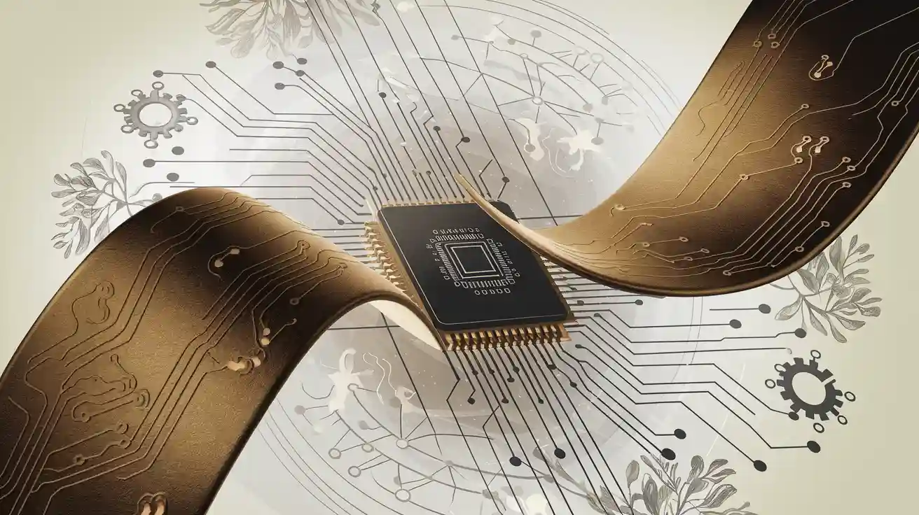
I have seen firsthand how ai flexible circuits drive new possibilities in AI projects. Flexible pcbs let me design hardware that adapts to new shapes and environments. When I work with ai flexible circuits, I notice how they boost both performance and creativity. I also see that flexible pcbs play a key role in making ai hardware smarter and lighter. However, integrating ai into the production of these circuits brings unique challenges that demand fresh solutions.
Key Takeaways
- Flexible circuits let designers create lightweight, bendable devices that fit tight spaces and improve AI hardware performance.
- Manufacturing flexible PCBs faces challenges like material sensitivity, precise patterning, and integrating diverse materials without defects.
- AI-driven tools and vision systems help monitor production, catch defects early, and maintain high quality and yield.
- Combining human expertise with AI builds trust, improves decision-making, and speeds up adoption of new technologies.
- Continuous innovation and AI support faster development, cost savings, and adaptable flexible circuits for future applications.
AI Flexible Circuits

Unique Properties
When I work with ai flexible circuits, I see how they change the way I design and build hardware. Flexible pcbs let me create devices that bend, twist, and fit into tight spaces. This flexibility supports new shapes and applications for ai accelerator pcbs. I often use materials like polyimide, fiberglass epoxy, ceramic, and PTFE. These materials give my pcb projects high-frequency capability, thermal stability, and low dielectric loss. I notice that high-frequency laminates from companies like Rogers Corporation help me maintain strong signal integrity, which is critical for hdi and microvia designs.
Note: Polyimide films, such as Kapton®, offer excellent thermal stability. I use them for high-density, energy-efficient flexible pcbs, especially in electric vehicle battery systems.
I rely on ai technologies to help me discover and optimize new materials. These tools speed up prototyping and improve recyclability. I also see that environmental rules, like U.S. TSCA and EU RoHS, push me to choose eco-friendly materials for my pcb designs.
Innovation in AI Projects
I have seen ai flexible circuits drive innovation in many real-world projects. For example, I worked on ai accelerator pcbs for wearable health monitors. These devices need flexible pcbs that can wrap around a wrist or fit inside clothing. The high-density interconnect and microvia structures let me pack more features into a small space. I also use ai to predict how materials will behave, which helps me avoid signal loss and improve reliability.
In automotive radar and 5G infrastructure, I use ai accelerator pcbs with advanced hdi and microvia layouts. These designs support fast data transfer and strong signal performance. I depend on ai-driven quality control during manufacturing to catch defects early and keep yields high. This approach lets me deliver high-performance, reliable flexible pcbs for the latest ai projects.
Challenges
Imaging and Material Sensitivity
When I design flexible pcb for ai hardware, I face several technical challenges. The materials I use, such as polyimide, are thin and sensitive. They react to heat, mechanical stress, and chemicals. Even a small temperature change, like 10°C, can shift the dimensions of the pcb by 0.02%. This shift affects alignment during imaging and can lead to defects. I must also create fine traces and tight tolerances, sometimes as small as 25 μm. Traditional imaging methods struggle to keep this precision on flexible substrates. I often see line breaks or shorts if the process is not perfect.
- Material sensitivity and flexibility make the pcb prone to deformation.
- High-resolution patterning is difficult, risking defects in hdi and microvia structures.
- Registration and alignment issues can degrade signal integrity, especially in multilayer designs.
- Handling thin substrates, often under 50 μm, leads to wrinkling or buckling during imaging.
To address these challenges, I use laser direct imaging and advanced photoresists. I rely on specialized equipment like vacuum tables and roll-to-roll systems to keep the substrate flat. I also control the environment to maintain stable temperature and humidity during imaging.
| Aspect | Description / Impact |
|---|---|
| Patterning Method | Controlled pyramid patterning via integrated dot-dispensing on flexible TPU-based composite substrates. |
| Structural Features | Uniform sensor arrays with porous microstructures, reinforced with CB/CF fillers. |
| Performance Improvements | Sub-milliNewton force resolution, high sensitivity, ultrafast response and recovery, excellent durability. |
| Functional Capabilities | Multimodal tactile sensing: pressure, sliding vector, trajectory velocity detection at micron-scale. |
| Material Contributions | TPU/CB/CF nanocomposites enhance electromechanical sensing and compliance. |
| Application Relevance | Enables robust real-time physiological monitoring, electronic skin, wearable electronics, robotics. |
| Reliability & Scalability | High uniformity and reliability; scalable array integration via dot-dispensing printing. |
High-resolution patterning directly improves the performance and reliability of flexible circuits. This is critical for advanced ai applications that need precise, multimodal tactile sensing.
Data and Model Issues
I often encounter data heterogeneity when integrating ai with flexible pcb manufacturing. Hybrid substrate strategies combine glass and organic layers. I must ensure reliable adhesion and thermal compatibility. New tooling and inspection methods are necessary to manage these diverse materials. Composite substrates allow me to build modular chiplet architectures, combining chips from different process nodes for optimized performance. Achieving ultra-dense, high-speed interconnects requires hybrid glass-core substrates, which are essential for hdi and high-performance computing processors.
- Aligning and bonding materials with different thermal and electrical properties can cause stress and failure.
- Heat dissipation becomes complex when I densely pack high-power chips.
- Signal interference, defect rates, and interconnect reliability present significant technical hurdles.
- Manufacturing yield and testing require advanced metrology and inspection at the nanometer scale.
- I use non-contact optical metrology and 3D inspection systems to measure alignment accuracy, bond integrity, and material stress.
Model interpretability also presents challenges. Deep learning models act as 'black boxes,' making it hard for me to understand their decisions. In federated learning environments, where data is decentralized, creating clear audit trails and explanations becomes even more difficult. Conventional explainable ai methods do not work well in these distributed settings. I must balance the need for explainability with data privacy, as detailed explanations can risk leaking sensitive information. Generating explanations also increases computational costs. Translating legal and ethical requirements into actionable ai policies remains a challenge. Symbolic and neurosymbolic ai approaches offer better clarity but are hard to integrate and scale.
Integration with Legacy Systems
Integrating flexible circuits and ai technologies with legacy manufacturing systems brings its own set of challenges. Legacy machine vision systems require complex calibration and programming. I often need third-party expertise, which increases costs and reduces flexibility. These systems are sensitive to environmental changes and rely on rigid, rules-based logic. This makes them bottlenecks in fast-paced, agile production environments.
- Legacy systems limit adaptability and slow down automated pcb assembly.
- Proprietary data formats and isolated systems make interoperability difficult.
- I have seen companies like Parker-Hannifin adopt open standards, such as the Asset Administration Shell (AAS), to enable seamless communication and integration across diverse equipment. This approach helps future-proof manufacturing operations and overcomes legacy system bottlenecks.
AI-powered vision systems help reduce hardware and setup costs. I can retrain ai models in-house, which improves responsiveness to production changes and reduces dependency on external consultants.
Operator Skepticism
Human factors play a big role in the adoption of ai in pcb assembly. Many operators feel skeptical about trusting ai recommendations. They worry that ai systems might overlook subtle defects or make decisions that do not align with their experience. I have noticed that building trust takes time. Operators need clear explanations and evidence that ai systems improve quality and efficiency.
- Operator skepticism can slow down the adoption of new technologies.
- Training and transparent communication help bridge the gap between human expertise and ai-driven processes.
- I encourage open feedback and involve operators in the development and testing of ai tools.
Challenges in PCB Assembly
The challenges in pcb assembly for flexible circuits are unique and complex. Flexible substrates require careful handling during every step of the process. I must manage laser drilling challenges, as drilling microvias in thin, flexible materials can cause deformation or misalignment. Maintaining signal integrity is critical, especially in hdi designs where traces are extremely fine and closely spaced.
- Automated pcb assembly systems must adapt to the delicate nature of flexible substrates.
- I use specialized pick-and-place machines and reflow ovens with precise temperature control to avoid damaging the pcb.
- Signal integrity issues arise if components are not placed accurately or if soldering introduces stress.
- I monitor the entire assembly process with advanced inspection systems to catch defects early and ensure high yield.
Signal integrity remains a top concern throughout the manufacturing and assembly process. I must ensure that every step, from imaging to final assembly, maintains the electrical performance required for advanced ai and hdi applications.
Solutions
AI-Driven Process Control
I have seen how AI-driven process control transforms manufacturing for flexible circuits. I use these solutions to monitor every step of the process, from material preparation to final assembly. Real-time data collection lets me spot trends and catch problems before they affect product quality. I rely on advanced pcb manufacturing techniques that use machine learning to adjust parameters automatically. This approach helps me maintain tight tolerances and high yield, even when working with sensitive materials.
I track key metrics to measure the success of AI integration in manufacturing. These include time savings, cost savings, error reduction rate, improved productivity, faster task completion, increased accuracy, compliance adherence, and scalability. I compare these metrics to the investment in AI to ensure that the solutions deliver real business value. I have seen production efficiency improve as manual labor costs drop and error rates decrease.
Vision Systems for Quality
I depend on vision systems for quality control in flexible pcb manufacturing. Automated inspection and testing play a crucial role in catching defects early. I use AI-powered vision systems that analyze images from multiple angles, detecting issues that human eyes might miss. These systems help me maintain the integrity of high-density interconnects and microvias, which are essential for ai accelerator pcbs.
Automated X-ray inspection systems, combined with hierarchical machine learning models, allow me to predict manufacturing outcomes with high accuracy. I can identify subtle anomalies and forecast potential failures before they impact the final product. This level of quality control ensures that I deliver high-quality pcbs with consistent performance.
Human-AI Collaboration
I believe that the best results come from combining human insight with AI-driven solutions. I involve operators in the development and testing of new tools. Their experience helps me fine-tune AI models and adapt them to real-world conditions. I encourage open feedback and transparent communication, which builds trust and speeds up adoption.
I train operators to use advanced pcb manufacturing techniques and automated inspection and testing systems. This approach bridges the gap between traditional skills and new technology. I see that human-AI collaboration leads to better decision-making and higher integrity in the manufacturing process.
Tip: Involve operators early in the process. Their feedback can reveal hidden issues and improve the effectiveness of AI solutions.
Predictive Maintenance
Predictive maintenance has become a game-changer in my manufacturing operations. I use AI to analyze equipment data and predict when machines need service. This approach reduces unplanned downtime and extends the life of expensive tools. I monitor vibration, temperature, and usage patterns to spot early signs of wear.
By scheduling maintenance only when needed, I save costs and keep production lines running smoothly. I have seen error rates drop and efficiency rise as a result. Predictive maintenance also supports the integrity of the manufacturing process, ensuring that every pcb meets strict quality standards.
Advanced Tools for Flexible PCBs
I use advanced AI tools to optimize layout and predict defects in flexible pcbs. Tools like PoLaRIS-PnR, Apollo placer, and LiDAR router, originally developed for photonic circuits, inspire my approach. These tools use AI-driven placement and routing algorithms to generate optimized layouts automatically. I see the potential for similar solutions in flexible pcb design, where constraints are complex and space is limited.
AI-based surrogate models and modular frameworks help me automate design tasks and prioritize simulation. I can test multiple design options quickly, improving efficiency and reducing time to market. I rely on advanced pcb manufacturing techniques to turn these designs into reality, using simulation to validate performance before production.
Industry reports confirm that AI-driven tools have transformed the pcb market. I now optimize complex layouts, predict manufacturing defects, and accelerate product development cycles. By analyzing manufacturing data, I detect subtle anomalies and predict equipment maintenance needs. This approach minimizes waste and rework, supporting the production of high-quality pcbs.
| Solution Area | Benefit for Flexible PCB Manufacturing |
|---|---|
| AI-Driven Process Control | Maintains tight tolerances, boosts yield |
| Vision Systems for Quality | Detects defects early, ensures product integrity |
| Human-AI Collaboration | Combines expertise, improves adoption |
| Predictive Maintenance | Reduces downtime, extends equipment life |
| Advanced AI Tools | Optimizes layout, predicts defects, speeds prototyping |
I always prioritize simulation in my workflow. This step lets me catch design flaws before they reach the production floor. I use simulation to test the electrical and mechanical performance of ai accelerator pcbs, ensuring that every design meets the highest standards.
With these solutions, I have improved production efficiency, reduced costs, and delivered reliable, high-quality pcbs. I see advanced pcb manufacturing techniques and AI-powered tools as the future of flexible circuit manufacturing.
Future Outlook
Trends in Flexible PCBs
I see flexible pcbs changing the way I approach electronics design. The demand for smaller, lighter, and more adaptable devices keeps growing. In my experience, new products like ultra-slim semiconductor bases and advanced hdi layouts help me achieve better flexibility and electrical performance. I notice that companies now use flexible pcbs in electric vehicles to manage electronic components in tight spaces. This trend improves both reliability and performance. Foldable displays and wearable health monitors also rely on these circuits. I expect the market to keep expanding as more industries adopt these solutions.
Evolving AI Integration
When I look at the next five years, I see companies using AI-powered tools to scan markets and predict trends. These tools help me make better decisions and adjust production quickly. I use AI to support dynamic pricing and improve supply chain management. Roll-to-roll printing, combined with automation, lets me produce flexible circuits faster and with fewer errors. I often work with partners from different industries to create new applications and customize products. The COVID-19 pandemic pushed me to adopt more digital and automated processes. Now, I focus on scalability to meet rising demand in healthcare, electric vehicles, and IoT devices. I see sustainability and personalized products becoming more important, so I use AI to stay agile and efficient.
Continuous Innovation
I believe continuous innovation drives progress in flexible circuit technology. I experiment with new materials like conductive polymers to improve grounding and flexibility. For wearables and medical devices, I use segmented or meshed ground structures and thin copper mesh layers. AI and simulation tools help me optimize grounding designs and predict electromagnetic interference. I see innovations in 3D PCB grounding and embedded components meeting the needs of compact, high-performance electronics. These advances make flexible circuits more reliable and adaptable. I always focus on scalability, so my solutions can grow with changing requirements. As I move forward, I expect flexible circuits to become even more efficient and tailored to dynamic environments.
I have seen flexible circuits and the right solutions spark real breakthroughs in technology projects. Success depends on how I address both technical and human challenges. Here are some proven strategies:
| Challenge Type | Strategy | Benefit |
|---|---|---|
| Technical | Use AI to optimize manufacturing | Faster development, lower costs |
| Human | Foster creativity and training | Teams adapt to new technologies |
When I combine innovation with practical steps, I unlock the full potential of flexible PCBs. I encourage you to keep exploring new ideas and solutions.
.png)
.png)
.png)
.png)

.png)

