


 2024-02-12
 BEST
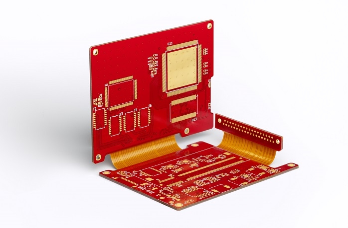
BESTFlex circuit prototyping plays a pivotal role in advancing electronic design, offering a versatile and adaptable solution for modern innovations. This process is essential for testing and refining concepts before full-scale production, ensuring precision and functionality. Mastering flex circuit prototyping is more than a technical skill; it is a gateway to unlocking new possibilities in electronic design. The ability to navigate the intricacies of flexible circuits empowers designers to push boundaries and create breakthrough technologies. This introduction sets the stage for exploring the significance of precise design, the flexibility inherent in flex circuits, and the integration of cutting-edge technology — all crucial elements in the journey towards mastering flex circuit prototyping and driving innovation in the ever-evolving field of electronic design.
Precision in Design
The Significance of Exact Design in Flex Circuits
Exact design serves as the bedrock for successful flex circuit prototyping, ensuring optimal functionality of electronic components within the confines of a flexible substrate. The intrinsic flexibility of these circuits necessitates meticulous attention to detail to mitigate challenges such as signal interference, mechanical stress, and material fatigue. The pursuit of precision in design is paramount for enhancing the reliability and longevity of the final product, critical considerations across diverse applications—from medical devices to consumer electronics.
Tools and Methods for Precision Mastery
Proficiency in specialized tools and techniques is essential for mastering the art of flex circuit prototyping. Tailored computer-aided design (CAD) software for flexible circuits facilitates precise layout and simulation, empowering designers to anticipate and address potential challenges early in the prototyping process. Laser cutting and advanced printing technologies contribute to fabricating intricate patterns with micron-level accuracy. Additionally, the integration of automated assembly processes ensures consistency and precision in component placement, further enhancing the overall reliability of flexible circuits.
Flexibility in Application
Harnessing the Versatility of Flexible Circuits
The inherent flexibility and adaptability of flex circuits represent a primary advantage, opening doors to a myriad of applications across diverse industries. From wearable technology to aerospace systems, flex circuits provide a solution where traditional rigid PCBs may prove inadequate. Their capacity to conform to complex shapes allows designers to seamlessly integrate electronics into products, fostering innovation and pushing the technological boundaries.
Design Considerations for Varied Applications
Effectively navigating the flexibility of circuits demands a profound understanding of the unique requirements of different applications. In medical devices, for example, circuit flexibility can be leveraged to create conformal and unobtrusive solutions for patient monitoring. In automotive applications, strategically incorporating flex circuits into compact and curved spaces optimizes functionality without compromising design. Designers must account for factors such as bending radius, material selection, and environmental conditions to tailor flex circuits for their intended applications, demonstrating the versatility of this technology across a spectrum of industries.
Best FPC's Cutting-Edge Technology
Integration of the Latest Technologies in Flex Circuit Prototyping
In the contemporary landscape, Flexible Printed Circuit (FPC) technology has become increasingly integral to precision equipment and daily life. BEST FPC strives to be a leading manufacturer of Flexible Circuits and Flexible Printed Circuit Boards in Asia, catering to global customers. The process begins with providing specific PCB prototyping data, enabling accurate quoting and product delivery cycle estimation based on the data, process requirements, and proofing quantity. Once both parties agree, a cooperation contract is signed, and the staff oversees order arrangement and production progress. The initial step involves material cutting according to customer-provided data and design requirements, tailoring the substrate material to the required size. Post-cutting, the substrate undergoes pretreatment to eliminate surface pollutants on the copper film, enhancing surface roughness for the subsequent film pressing process.
Advancements in Materials and Manufacturing Processes
- Flexible PCB Structure Layer Formation:
Layer formation involves pressing the inner layer of the PCB, affixing an anti-corrosion dry film to the copper surface via hot pressing. After exposure and development, the image on the original negative film transfers to the photosensitive base plate. Unreacted dry film is washed away, leaving the chemically reacted film as the anti-corrosion protective layer during corrosion. The exposed copper is then corroded to form the required inner line pattern.
- Troubleshooting FPC Defects or Errors:
Post-etching, the anti-corrosion layer is peeled off to expose the circuit diagram. Inner layer inspection follows, identifying and addressing abnormal PCBs. The process involves punching through CCD, creating positioning and rivet holes for detection. AOI inspection and VRS confirmation utilize light reflection principles to detect abnormalities, with VRS confirming AOI-detected anomalies manually.
- Multilayer Flex Circuit Board Proofing:
After confirming the inner board, the next steps involve pressing copper foil, film, and oxidized inner circuit board into a multilayer board. The copper surface undergoes browning and roughening to increase resin wetting, avoiding adverse reactions. Riveting prevents layer sliding during subsequent processes. Lamination combines pre-laminated layers into a multi-layered plate, pressed through hot pressing to form the final multi-layered plate.
Case Studies
Successful Applications of Mastered Flex Circuit Prototyping
Mastering flex circuit prototyping is exemplified through the successful application of up to 10 layers in Flex PCB prototyping. Following the pressing process, holes are drilled for inter-layer connections. Electroplating ensures metallization of non-conductive parts on hole walls, with subsequent removal of glue slag exposing copper holes for interconnection. Outer layer treatment, film pressing, exposure imaging, and secondary electroplating follow, tailoring copper thickness to customer specifications. Tin stripping, line etching, AOI inspection, and VRS confirmation complete the outer layer. The complexity increases with the number of layers, necessitating multiple pressing times and processes.
Unique Solutions and Innovations
Ensuring the integrity of flex circuit samples involves anti-welding measures for protection and insulation. Silk screen characters are applied for maintenance and identification. The final step includes surface processing and manual testing, with some customers opting for additional special processes tailored to their specific requirements.
Future Trends
Emerging Trends in Flex Circuit Technology
Flex circuit technology is on the cusp of transformative changes. Emerging trends include advancements in material science, enabling the development of more robust and flexible substrates. Innovations in conductive materials and printing technologies are poised to enhance the performance and reliability of flex circuits. Integration with Internet of Things (IoT) devices and wearables is becoming more prevalent, expanding the applications of flex circuits beyond traditional boundaries.
Anticipated Developments and Their Impact on Prototyping
Anticipated developments in flex circuit technology are expected to significantly impact the prototyping landscape. Rapid advancements in additive manufacturing techniques may lead to more efficient and cost-effective prototyping processes. The integration of artificial intelligence (AI) and machine learning into design and testing phases could streamline the prototyping workflow, accelerating innovation. Additionally, the continued miniaturization of electronic components and the exploration of novel materials may open new possibilities for compact and high-performance flex circuit designs, shaping the future of electronic prototyping.
Final Words
Mastering flex circuit prototyping is a journey marked by precision, adaptability, and technological advancements. The importance of precise design and the integration of cutting-edge tools are evident in ensuring the optimal functionality of electronic components. The showcased case studies exemplify the versatility of flex circuits, from complex multi-layered prototypes to specialized solutions. As we look towards the future, emerging trends in flex circuit technology promise transformative changes, with innovations in materials, manufacturing processes, and the integration of IoT. Anticipated developments signal a dynamic landscape, with the potential for more efficient and intelligent prototyping processes. Flex circuit prototyping is not just a technical process but a catalyst for driving innovation in electronic design, shaping the way we interact with technology in the years to come.
.png)
.png)
.png)
.png)

.png)

