


 2023-03-22
 BEST
BESTStandard flex stack up for 1 layer flex pcb:
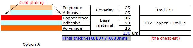
This is the simplest flex pcb. Generally, base material and adhesive and copper foil are used as raw materials, or protective film and adhesive are used. Firstly, copper foil needs to be etched to get traces required. Protective film needs to be drilled to expose pad. Both are combined by using rolling process after cleaning, then the exposed pad should be electroplated with gold or tin for protection. In this way, the flex PCB is finished and can be punched into small flex pcb.
Standard flex stack up for 2 layers flex pcb:
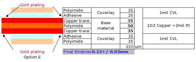
When the traces of flex pcb are too complicated, the 1 layer flex pcb can not meet the needs of wiring, or needs copper foil for grounded shield, 2 layers flex pcb or multilayers flex pcb can be used.
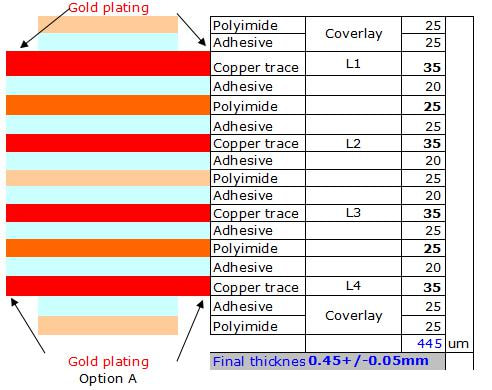
Standard flex stack up for multilayers flex pcb:
The via holes are added to make multilayers flex pcb different from 1 layer flex pcb, so that copper foil in each layer can be connected. Generally, for base materials and adhesive and copper foil, the first processing technique is to make via holes. The base materials and copper foil should be drilled firstly and then electroplated with copper of certain thickness after cleaning. Thus the via holes are finished. The subsequent manufacturing techniques of multilayers flex pcb are almost the same with 1 layer flex pcb.
For example, here is the standard flex stack up for 4-layer flex pcb
There may be some differences among the stackup for 1 layer flex pcb, 2 layers flex pcb and multilayer flex pcb, but similarities also exist among many manufacturing techniques of flex pcb. Different
.png)
.png)
.png)
.png)

.png)

