


 2023-07-12
 BEST
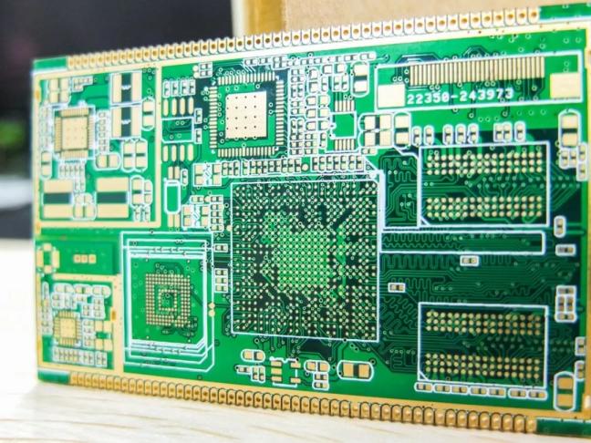
BESTMultilayer bendable printed circuit boards (PCBs) have gained significant popularity in various industries due to their flexibility and adaptability to complex designs. These specialized PCBs offer unique advantages in applications such as wearable devices, medical equipment, automotive electronics, and more. However, the manufacturing process of multilayer bendable PCBs comes with its own set of challenges. In this blog, we will explore the requirements and hurdles faced by manufacturers, with a focus on the Best FPC Technology Company.
Requirements for Multilayer Bendable PCBs: Why is Multilayer Bendable PCB Used?
Why is multilayer bendable PCB used? To produce high-quality multilayer bendable PCBs, manufacturers need to meet several crucial requirements. These include:
1. Flexibility: The PCBs must be able to withstand repeated bending and flexing without compromising their electrical and mechanical performance.
2. Reliability: The boards should maintain signal integrity and electrical continuity even in harsh environments or when subjected to extreme temperatures, vibrations, and other stressors.
3. Miniaturization: As devices become smaller and more compact, multilayer bendable PCBs must support higher circuit density and component integration, requiring manufacturers to overcome space constraints.
4. Cost-effectiveness: While maintaining quality, manufacturers need to optimize the production process to minimize costs and provide competitive pricing for customers.
Hurdles Faced by Manufacturers: Why is Multilayer Bendable PCB Used?
1. Material Selection and Compatibility:
Selecting suitable materials is critical in the manufacturing of multilayer bendable PCBs. The chosen materials must exhibit excellent flexibility, high thermal stability, and compatibility with other materials and processes involved. Manufacturers face the challenge of finding the right combination of materials that can withstand bending stress while ensuring reliable electrical connections.
2. Complex Design and Assembly:
Multilayer bendable PCBs often involve intricate designs with multiple layers, fine traces, and tiny components. Achieving the desired level of miniaturization and ensuring proper alignment during assembly can be a complex task. Manufacturers need to develop advanced manufacturing techniques, including precise positioning and bonding methods, to handle intricate designs effectively.
3. Manufacturing Process Optimization:
Efficiently producing multilayer bendable PCBs at scale is another significant challenge. Balancing flexibility, reliability, and cost-effectiveness requires optimizing various stages of the manufacturing process, such as surface treatment, lamination, etching, and solder mask application. Manufacturers like Best FPC Technology Company continuously invest in research and development to improve production efficiency and reduce lead times.
4. Quality Control and Testing:
Ensuring the quality and reliability of multilayer bendable PCBs is crucial to meet customer expectations. Rigorous quality control measures and testing procedures are essential throughout the manufacturing process. Manufacturers need to implement advanced inspection techniques, such as automated optical inspection (AOI), X-ray inspection, and electrical testing, to identify and rectify any potential defects.
Best FPC Technology Company: Addressing Industry Challenges:
As a leading manufacturer in the field, Best FPC Technology Company has been at the forefront of addressing the challenges associated with multilayer bendable PCBs. They have implemented several strategies to overcome these hurdles:
1. Research and Development: Best FPC invests heavily in research and development to explore new materials, advanced manufacturing processes, and innovative designs. This commitment allows them to continually enhance their capabilities and offer cutting-edge solutions to their customers.
2. Collaboration with Material Suppliers: Best FPC works closely with material suppliers to identify and evaluate new materials suitable for multilayer bendable PCBs. This collaborative approach ensures access to the latest material technologies and enables the company to select the most reliable and compatible options.
3. Advanced Manufacturing Techniques: Best FPC utilizes state-of-the-art manufacturing techniques, including precise laser drilling and etching, to achieve the desired levels of flexibility and miniaturization. Their expertise in assembly processes enables them to handle complex designs efficiently.
4. Quality Assurance: Best FPC has stringent quality control measures in place to ensure the reliability and performance of its multilayer bendable PCBs. They employ advanced testing methodologies, including 100% visual inspection, AOI, X-ray inspection, and electrical testing, to deliver products of the highest standards.
Modern Electronics: Why is Multilayer Bendable PCB Used?
With the rise in demand for exceptional circuit board designs, manufacturers have discovered and incorporated the use of bendable multilayer PCBs into their production methods. Such a major technological advancement has changed the way electronic components are created, now resulting in convenient and smaller sizes which were unheard of. Leading manufacturing company, Best FPC Technology Company, has been a significant part in developing these bendable boards.
1. Enhanced Flexibility: Empowering Design Possibilities
Multilayer bendable PCBs offer unparalleled flexibility, allowing electronic devices to conform to unconventional shapes and contours. By using flexible materials such as polyimide, these PCBs can be bent, twisted, and folded without compromising their functionality. This remarkable attribute provides designers with a newfound freedom to create innovative and compact products that meet the demands of contemporary consumers. From wearable technology to medical devices and automotive electronics, the flexibility of multilayer bendable PCBs has opened up a world of design possibilities.
2. Space Optimization: Achieving Compact Form Factors
In today's increasingly miniaturized electronic devices, space optimization is crucial. Multilayer bendable PCBs excel in this aspect by eliminating the need for bulky connectors and reducing the overall size of the circuitry. The ability to bend and fold the PCBs allows them to fit into tight spaces, enabling the creation of slimmer and more compact devices. This advantage has significantly contributed to the miniaturization of smartphones, tablets, and other portable gadgets, enhancing their portability and user experience.
3. Improved Signal Integrity: Minimizing Interference
Another key advantage of multilayer bendable PCBs is their ability to maintain excellent signal integrity. By utilizing multiple layers, designers can implement shielding and impedance control techniques more effectively, resulting in reduced electromagnetic interference (EMI) and improved signal transmission. The flexible nature of these PCBs also helps mitigate mechanical stress, which can be a significant factor in signal degradation. This enhanced signal integrity is particularly critical in applications such as high-speed data transmission, where maintaining the integrity of the signal is paramount.
4. Reliability and Durability: Withstanding Harsh Environments
In many industries, electronic devices are exposed to harsh and demanding environments. Multilayer bendable PCBs, constructed using robust materials and advanced manufacturing techniques, offer exceptional resistance to vibration, shock, and temperature fluctuations. This durability makes them well-suited for applications in the automotive, aerospace, and military sectors, where reliability is of utmost importance. Additionally, the elimination of rigid connectors and solder joints, which are prone to failure under stress, further enhances the overall reliability of these PCBs.
5. Cost-Effectiveness: Streamlining Manufacturing Processes
Contrary to conventional belief, multilayer bendable PCBs can actually contribute to cost savings in the long run. The flexibility of these PCBs simplifies the assembly process, reducing the number of components required and minimizing labor costs. Additionally, their compact form factor allows for more efficient use of materials, reducing waste and lowering production expenses. Moreover, their durability and resistance to environmental factors contribute to a longer product lifespan, reducing maintenance and replacement costs.
Conclusion
Multilayer bendable PCBs present a range of challenges for manufacturers, demanding expertise in material selection, design, manufacturing process optimization, and quality control. Best FPC Technology Company, as a leading manufacturer in the industry, addresses these challenges through continuous innovation, collaboration with suppliers, and advanced manufacturing techniques. With their commitment to excellence, they play a vital role in meeting the growing demands for multilayer bendable PCBs in various industries, enabling the development of next-generation electronic devices.
.png)
.png)
.png)
.png)

.png)

