


 2023-11-13
 BEST
BESTA 4-layer rigid-flex PCB stack-up merges the resilience of rigid PCBs with the versatility of flexible circuits, encompassing four conductive layers for intricate design capabilities. Essential in compact and high-performance electronics, this hybrid provides enhanced durability and space efficiency, pivotal in cutting-edge electronic advancements.
What is Rigid-Flex PCB?
Understanding Rigid-Flex PCBs
Rigid-flex Printed Circuit Boards (PCBs) combine the best of both rigid and flexible circuit technologies. They consist of multiple layers of flexible circuit substrates attached to rigid boards, creating a hybrid PCB that can be designed to fit into space-constrained applications while providing a higher density of component assembly. This innovative solution offers a dynamic flexing capability, enabling the board to conform to desired shapes during application or installation.
Benefits Of Traditional PCBs
The primary advantage of rigid-flex PCBs is their versatility. They can be folded or continuously flexed, which saves space and reduces the need for connectors and wiring harnesses, thereby enhancing reliability. This reduction in mechanical bulk also translates into lighter and more streamlined designs. Furthermore, the integration of multiple PCB assemblies into a single rigid-flex PCB enhances the durability of the overall electronic package, as it minimizes the interconnection problems that can plague traditional PCB designs.
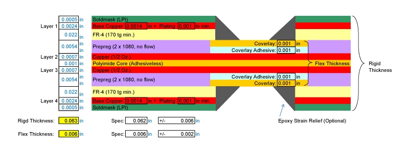
Composition of the 4-layer Stackup
Layer 1: Top Layer
The top layer of a rigid-flex PCB typically consists of copper foil, which is the conductive material where components and traces are placed. This layer is essential for the distribution of signals and power throughout the PCB.
Layer 2: Prepreg
Beneath the copper foil is the prepreg layer, a fiberglass material impregnated with resin that, when heated, acts as the adhesive to bind layers together. It provides insulation between the copper and core layers and adds structural integrity to the PCB.
Layer 3: Core
The core layer is usually made of a rigid fiberglass material similar to what is found in traditional rigid PCBs. It provides the main structural rigidity to the board and carries copper circuits that may not need to flex.
Layer 4: Bottom Layer
The bottom layer mirrors the top, with another layer of copper foil. It completes the electrical circuit and provides a ground plane or additional routing area for signal traces.
Materials Used in Each Layer
The materials selected for each layer are crucial for the board’s function. The copper used is often annealed to improve flexibility; the prepreg is formulated for resilience under thermal cycling; and the core is chosen for its mechanical stability and dielectric properties.
Role of Each Layer in the Stackup
Each layer in the stack serves a distinct purpose:
- The copper layers carry the electronic signals to and from components.
- The prepreg acts as an insulating adhesive, maintaining the integrity of signal paths and providing structural support.
- The core gives the PCB its rigidity where necessary and contributes to the overall thickness and stability of the board.
Design Considerations
Electrical Requirements
Designers must consider the electrical requirements, including impedance control, signal integrity, and power distribution. Rigid-flex PCBs can have complex circuits, requiring careful planning of trace layouts to prevent noise, crosstalk, and other electromagnetic interference (EMI) issues.
Mechanical Constraints
Mechanical constraints include the bend radius of the flex regions and the overall board thickness. These factors are critical when the PCB must fit into a tight space or when it needs to flex during operation or installation.
Thermal Management
Thermal management is another crucial aspect, especially for high-power applications. Designers must consider the thermal profile of the assembly, including the placement of heat-generating components and the use of thermal relief features such as vias and heat sinks.
Manufacturing Process
The production of a 4-layer rigid-flex PCB is a complex procedure that demands precision and careful planning. Here is a step-by-step overview:
- Design and Layout: Initially, PCB designers develop a detailed blueprint using CAD software, which specifies all electrical connections between components.
- Material Selection: Appropriate substrate materials for both the rigid and flexible parts of the PCB are selected. Common materials include polyimide for flexibility and FR4 for rigidity.
- Circuit Printing: The circuit pattern is printed onto each layer. For rigid areas, this involves laminating copper sheets to the substrate and etching away excess material. For flexible sections, it involves using a photolithographic process.
- Layer Stacking: The individual layers are stacked in the correct order. Adhesives and insulation materials are used to bond the layers, with careful alignment to ensure connectivity.
- Drilling and Plating: Holes are drilled to create vias, and the board is plated with copper to establish connections between the layers.
- Etching and Lamination: Additional etching is performed if necessary, followed by lamination to protect the circuitry.
- Assembly: Components are added to the board, often using surface mount technology for precision.
- Testing: Finally, the board is rigorously tested for functionality and reliability.
Challenges in manufacturing rigid-flex PCBs include maintaining alignment during lamination, ensuring the quality of the plated through-holes, and managing the different thermal expansion rates of materials. Solutions involve advanced machinery for precise alignment, chemical plating for quality through holes, and careful material selection to mitigate thermal issues.
Applications of 4-Layer Rigid-Flex PCBs
Rigid-flex PCBs are utilized in a wide range of applications due to their versatility:
- Consumer Electronics: In smartphones and wearable devices where space is at a premium, a 4-layer rigid-flex PCB allows for a compact and flexible design.
- Medical Devices: For highly sensitive medical equipment like pacemakers, the reliability and precision of these PCBs are crucial.
- Aerospace and Defense: Rigid-flex PCBs are used in satellites and avionics for their ability to withstand extreme conditions and vibrations.
- Automotive: Modern vehicles, with their increasing electronic content, rely on rigid-flex PCBs for everything from control systems to sensors.
Advantages of 4-Layer Rigid-Flex PCBs
Enhanced Durability and Reliability: The combination of rigid and flexible layers allows these PCBs to withstand bending and movement, reducing the risk of breakage in applications involving motion or stress.
Improved Signal Integrity
Multiple layers enable designers to separate power and ground planes, which reduces electromagnetic interference and enhances signal integrity.
Space and Weight Reduction
Rigid-flex PCBs can replace multiple traditional rigid boards and connectors, leading to a considerable reduction in space and weight—essential for modern, lightweight devices.
The integration of rigid and flexible technologies in a 4-layer stackup offers a sophisticated solution for today’s high-demand electronics, providing unmatched flexibility, reliability, and performance in an array of industries.
CONCLUSION
The 4-layer rigid-flex PCB stackup solution represents a pinnacle of electronic component design, blending flexibility with robustness to meet the exacting demands of modern technology. This optimal integration underpins the functionality of cutting-edge devices across various industries, offering a compact, reliable, and high-performance solution that is essential for innovation in the electronics sector.
.png)
.png)
.png)
.png)

.png)

