


 2026-03-06
 BEST
BESTTable of Contents
- Understanding the 3+N+3 HDI Rigid-Flex Architecture
- Core Stack-Up Design Rules for 3+N+3 HDI Rigid-Flex PCBs
- Microvia Engineering and Reliability Design
- Material Selection and Signal Integrity Optimization
- Industry Applications in the United States and Lebanon
- Key Factors Engineers Must Consider When Designing 3+N+3 HDI Rigid-Flex PCBs
- FAQ: 3+N+3 HDI Rigid-Flex PCB Design
- Why BESTFPC Is a Trusted Supplier for Advanced HDI Rigid-Flex PCBs
- Conclusion
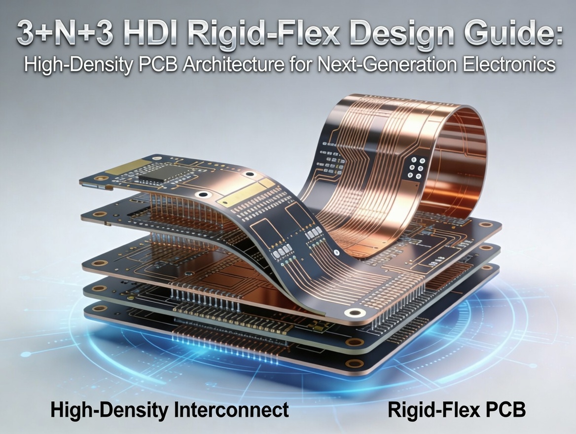
Understanding the 3+N+3 HDI Rigid-Flex Architecture
High-Density Interconnect (HDI) technology has become a critical foundation for advanced electronic systems, especially when engineers must integrate high-speed processing, compact packaging, and complex signal routing within a limited board area. Among various HDI stack-up configurations, 3+N+3 HDI rigid-flex architecture represents one of the most advanced designs used in modern electronics.
The structure refers to three sequential buildup layers on the top and bottom of a core layer stack (N). This configuration enables designers to route complex signals across multiple layers while maintaining compact dimensions. A typical 3+N+3 HDI stack-up may include 12–16 layers, combining rigid sections for component mounting and flexible sections for dynamic interconnections.
Rigid-flex technology integrates flexible polyimide circuits with rigid FR-4 substrates into a single board, eliminating connectors and cables between boards. This design reduces weight, improves reliability, and allows three-dimensional circuit routing in compact devices.
In a 3+N+3 HDI stack-up:
- Outer layers contain microvias connecting adjacent layers.
- Intermediate buildup layers use stacked or staggered microvias.
- Core layers handle power distribution and signal reference planes.
Laser-drilled microvias used in HDI designs can reach diameters as small as 75 µm, enabling significantly higher routing density than traditional through-hole PCBs.
For complex electronics such as AI modules, aerospace sensors, or medical imaging equipment, this structure allows engineers to integrate high-pin-count BGAs, controlled impedance routing, and high-speed differential signals within a compact footprint.
Because of its complexity, successful 3+N+3 HDI rigid-flex design requires close collaboration between PCB designers and manufacturers to ensure manufacturability, reliability, and cost efficiency.
Core Stack-Up Design Rules for 3+N+3 HDI Rigid-Flex PCBs
Designing a reliable 3+N+3 HDI rigid-flex PCB begins with careful stack-up planning. The stack-up determines electrical performance, signal integrity, and manufacturability.
The most common configuration includes:
- 3 HDI buildup layers (top)
- N core layers
- 3 HDI buildup layers (bottom)
This architecture enables high-density routing for advanced components such as 0.5 mm pitch BGA or finer packages.
HDI Layer Structure
A typical 14-layer 3+N+3 HDI rigid-flex stack-up may include:
Top layers
- L1 signal
- L2 microvia buildup
- L3 microvia buildup
Core layers
- L4–L11 power and signal layers
Bottom layers
- L12 microvia buildup
- L13 microvia buildup
- L14 signal
Microvias connect adjacent layers, while buried vias link internal layers for efficient signal routing.
IPC Design Standards
Several IPC standards guide HDI rigid-flex design:
- IPC-2226 – HDI structure design guidelines
- IPC-6012 – performance and reliability requirements
- IPC-TM-650 – thermal stress testing methods
These standards specify critical parameters such as:
- Maximum microvia aspect ratio of 1:1
- Minimum trace width 50–75 µm
- Minimum annular ring 0.02 mm
By following these standards, designers can ensure that the PCB meets reliability requirements for aerospace, automotive, and medical applications.
Microvia Engineering and Reliability Design
Microvias are the defining feature of HDI technology and play a crucial role in the performance of 3+N+3 rigid-flex PCBs.
Unlike traditional mechanical vias, microvias are created using laser drilling, allowing extremely small diameters and short interconnection paths.
Microvia Size and Structure
Typical HDI microvia parameters include:
| Parameter | Typical Value |
|---|---|
| Microvia diameter | 75–150 µm |
| Capture pad | ≥100 µm larger than via |
| Aspect ratio | ≤1:1 |
| Annular ring | ≥0.02 mm |
These parameters ensure proper copper plating and mechanical stability.
Stacked vs Staggered Microvias
Engineers may choose between two microvia strategies:
Stacked microvias
- allow vertical interconnections
- maximize routing density
- require copper filling and plating
Staggered microvias
- reduce thermal stress
- improve reliability in high-temperature environments
Stacked vias typically should not exceed two stacked levels to maintain long-term reliability.
Additionally, microvias should be positioned at least 1 mm away from flex bending areas to prevent cracking during mechanical stress.
Proper microvia design ensures that the PCB can survive thousands of thermal cycles and mechanical stresses without failure.
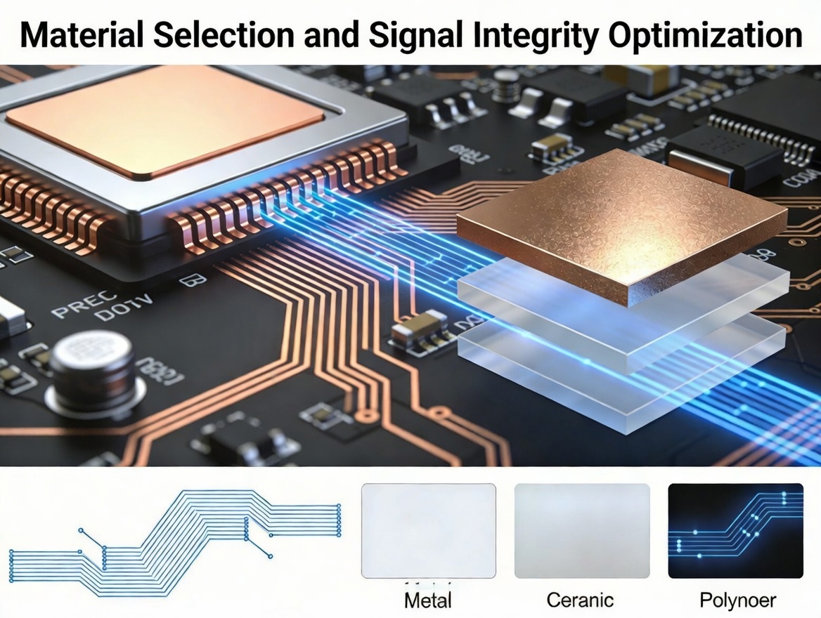
Material Selection and Signal Integrity Optimization
Material selection plays a vital role in achieving optimal electrical performance in HDI rigid-flex circuits.
Rigid sections typically use high-Tg FR-4 laminates, while flexible sections use polyimide substrates that support repeated bending cycles.
Key Material Properties
Important parameters include:
- dielectric constant (Dk)
- dissipation factor (Df)
- coefficient of thermal expansion (CTE)
For high-speed applications such as 5G or AI computing systems, designers may use low-loss materials such as Rogers laminates to maintain signal integrity at high frequencies.
Controlled Impedance Design
High-speed circuits require strict impedance control. Typical rigid-flex impedance tolerance is around ±6%, depending on stack-up design and manufacturing precision.
Engineers often use techniques such as:
- differential pair routing
- ground plane shielding
- impedance simulation
to maintain signal quality and reduce electromagnetic interference.
Industry Applications in the United States and Lebanon
Different industries rely on HDI rigid-flex PCBs for different reasons.
Understanding these requirements helps engineers choose the right design architecture.
Aerospace and Defense
In the United States, aerospace electronics require extremely high reliability and resistance to vibration and temperature fluctuations.
3+N+3 HDI rigid-flex boards are used in:
- avionics systems
- satellite communication modules
- navigation electronics
These systems benefit from reduced connectors and improved mechanical reliability.
Medical Electronics
Medical devices such as endoscopes and imaging systems rely on rigid-flex PCBs for compact design and high reliability.
The combination of HDI routing and flexible circuits enables:
- smaller device size
- higher component density
- improved signal transmission
Telecommunications and Data Infrastructure in Lebanon
Lebanon’s telecommunications sector continues to modernize its infrastructure, increasing demand for compact and high-performance electronics used in:
- telecom base station modules
- network routers
- RF communication systems
HDI rigid-flex boards provide the necessary density for advanced RF routing and signal integrity.
Consumer Electronics
In both the U.S. and Middle East markets, rigid-flex PCBs are widely used in:
- wearable electronics
- smart devices
- IoT products
These applications require high component density and flexible mechanical design.
Key Factors Engineers Must Consider When Designing 3+N+3 HDI Rigid-Flex PCBs
Several design factors determine whether a 3+N+3 HDI rigid-flex PCB will perform reliably.
Manufacturing capability
Designers must confirm that the manufacturer supports microvias as small as 0.075 mm and stacked via technology.
Thermal reliability
The PCB must withstand repeated temperature cycles without microvia cracking or layer delamination.
Mechanical stress
Rigid-flex transitions must be carefully designed to prevent stress concentration.
Signal integrity
High-speed signals require controlled impedance and proper grounding strategies.
Close collaboration with an experienced manufacturer during the design stage significantly reduces risk and shortens development time.
FAQ: 3+N+3 HDI Rigid-Flex PCB Design
What does 3+N+3 mean in HDI PCB design?
It refers to three buildup layers on the top and bottom of the core PCB layers, enabling high-density routing and microvia interconnections.
Why are microvias important in HDI rigid-flex PCBs?
Microvias allow high routing density and short signal paths, improving electrical performance and reducing board size.
What industries use 3+N+3 HDI rigid-flex PCBs?
Common industries include aerospace, medical electronics, telecommunications, and advanced consumer devices.
Why BESTFPC Is a Reliable Manufacturer for HDI Rigid-Flex PCBs
For companies designing advanced electronic systems, selecting the right PCB manufacturing partner is crucial.
BESTFPC provides:
- advanced HDI rigid-flex manufacturing technology
- precision laser microvia drilling
- multilayer rigid-flex PCB production
- strict reliability testing and quality control
Internal links recommended for SEO:
- Rigid-Flex PCB Manufacturing
- HDI PCB Technology Guide
- Flexible PCB Prototyping
With extensive experience in high-density PCB fabrication, BESTFPC supports engineers in developing reliable designs for complex electronic applications.
Conclusion
The 3+N+3 HDI rigid-flex architecture represents one of the most advanced PCB technologies available today.
By combining microvia interconnects, multilayer stack-ups, and flexible circuit integration, engineers can achieve unprecedented circuit density and performance.
However, successful implementation requires careful attention to:
- stack-up planning
- microvia reliability
- material selection
- signal integrity
Working with an experienced manufacturer such as BESTFPC ensures that these complex designs can be manufactured reliably and efficiently.
.png)
.png)
.png)
.png)

.png)

