


 2022-11-08
 BEST
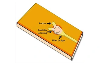
BESTThe materials used to manufacture flexible circuits typically contain acrylic adhesive. When heated, this acrylic adhesive can become soft and pliable. However, when designed properly, these circuits are extremely dependable. Making the pads as large as possible is key. On single circuits, we recommend the use of anchors or spurs. During dynamic bending, anchors help stabilize the outer layer. Flex PCBs with multi-layers do not have any issues with adhesives.
BEST TECH also highly recommends using teardrops on all flexible PCBs. Teardrops can reduce and even eliminate potential stress concentration points on the PCB.
Elongated Pads
Elongated Pads can increase the annular ring in tight geometry and also increase terminal area bond strength.
Pads
Whenever possible, design pads larger than the access holes. If space is critical, use hold-down tabs. Hold-down tabs are especially important for single-layer circuits, because a single-layer circuit does not have the added strength of plated through- holes. A variety of hold-down tab designs are available.
Pad fillets
Pad fillets improve etched yield and material strength. Fillets are appropriate when the pad diameter is greater than the connecting strand width. Acute angles at the interface between conductors and pads are to be avoided by using fillets to minimize the concentration of stress at the interface.
Pad Size vs. Hole Size Calculation
The area where Artwork designs fail most to allow enough processing tolerance to meet the minimum annular ring is “pad size” calculation. BEST TECH uses the formula from MIL-STD-2118 to calculate the minimum pad size for the required hole size. The formula is as follows:
Minimum Pad Size = A + 2B +2C(when required) + D
A = Maximum diameter of the drilled hole for internal lands and finished hole for external Lands.
B = Minimum annular ring required
C = Maximum allowance for etchback (when required)
D = Standard Fabrication Allowance. This was determined by statistical survey, which considers tooling and process variations required to fabricate boards.
** BEST TECH will accept all Artwork down to reduced productivity **
STANDARD FABRICATION ALLOWANCES
Example A: Double Sided Circuit with .035 +/-.003 hole size
|
Biggest Board Dimension |
ALLOWANCES (INCHES) |
||
|
Preferred |
Standard |
Reduced Productibility |
|
|
Up to 12 Inches |
0.28 |
0.02 |
0.012 |
|
12-18 Inches |
0.034 |
0.024 |
0.016 |
|
>18 Inches |
Drawing tolerances must reflect bend and fold allowances between component mounting rigid areas |
||
Minimum Pad Size = .040 (drill size) + .010 (2 x .005 annular ring) + 0 (no etchback) + .012 (reduced productibilty factor) or = .062”
Example B: Multi-layer Circuit with .035 +/- .003 hole size
Minimum Pad Size = .041 (drill size) + .004 (2 x .002 annular ring) + .006 (2 x .003 max. etchback) + (Internal Layer) .012 (reduced productibility factor) or = .063”
.png)
.png)
.png)
.png)

.png)

