


Thin-film Ceramic Circuit Board Rapid Prototype For Energy Storage System


Board Thickness: 0.635mm
Conductor: 0.1umTi+0.2umPt
Solder Mask: N/A
Silkscreen: N/A
Surface Finishing: N/A
Application: Energy Storage System
.png)
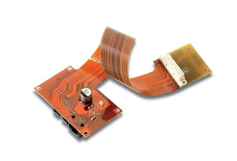
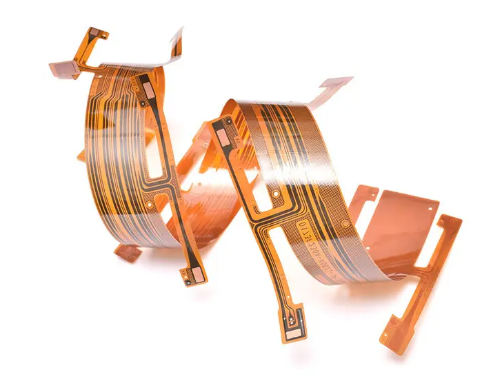
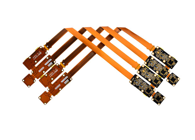
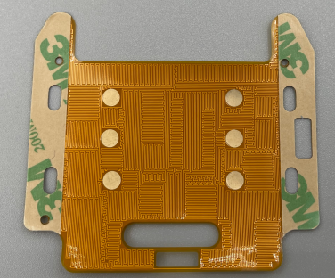
Products
.png)
.png)
.png)
.png)
.png)

.png)
| Item1 | Thin Film Capabilities | |||||
|---|---|---|---|---|---|---|
|
Layer Count |
2 Layers |
|||||
|
Max Board Dimension |
138*190mm |
|||||
|
Min Board Thickness |
0.25mm |
|||||
|
Max Board Thickness |
2.0mm |
|||||
|
Conductor Thickness |
2um - 200um |
|||||
|
Min Line Width/Line Space |
6/8mil (0.15/0.20mm) |
|||||
|
Substrate Type |
AI203,ALN, Zro2, Si3N4 |
|||||
|
Substrate Thickness |
0.25, 0.38, 0.50, 0.635, 0.80,1.0, 1.25, 1.5, 2.0mm |
|||||
|
Min Hole Diameter |
4mil (0.1mm) |
|||||
|
Min Hole Spacing |
NPTH: 16mil (0.30mm); PTH: 20mil (0.5mm) |
|||||
|
Min PAD Ring(Single) |
3mil (0.075mm) |
|||||
|
PTH Wall Thickness |
4mil (10um) |
|||||
|
Min Solder PAD Dia |
6mil (0.15mm) |
|||||
|
Min Soldermask Bridge |
6mil (0.15mm) |
|||||
|
Min BAG PAD Margin |
8mil (0.20mm) |
|||||
|
PTH/NPTH Dia Tolerance |
PTH: ±4mil (0.1mm) ; NPTH: ±2mil (0.05mm) |
|||||
|
Hole Position Deviation |
± 4mil (0.1mm) |
|||||
|
Outline Tolerance |
Laser: +0.2/0.05mm;Die Punch: +0.25/0.20mm |
|||||
|
Line Width/Spac Tolerance |
+1mil (0.025mm) |
|||||
|
Surface Treatment |
OSP/ENIG/ENEPIG |
|||||
|
Thermal Stress |
15 min @ 350 C |
|||||
| Item2 | Attribute | ||
|---|---|---|---|
|
Brand |
CeramTec / GTT / Huaqing / Laird / Maruwa / Rogers / Toshiba |
||
|
Base Material |
AI203 / ALN / BeO / SiO2 |
||
|
Base Material Thickness (exclude conductor) |
0.20mm / 0.25mm / 0.30mm / 0.38mm / 0.50mm / 0.635mm/ 0.76mm / 0.80mm / 1.0 mm/ 1.2 mm / 1.5mm / 2.0 mm |
||
|
Thermal Conductivity |
24w / 27w / 170w / 200w / 240W |
||
|
Soldermask Type |
Glass glaze , Soldermask oil (white , black , green , blue , yellow , red) |
||
|
Tg Value |
200 / 250 / 300 / 400 / 500 / 600 / 700 / 800 |
||
|
Halogen Free |
Yes (optional) |
||
|
Breakdown Voltage |
11 - 34 KV/ |
||
|
Dielectric Constant (MHZ) |
9 - 10 |
||
|
Water Absorption |
0% |
||
|
ROHS |
Yes |
||
|
Flammability |
94V-0 |
||
|
Thermal Conductivity (W/m.K, or W/m.C) |
Al2O3: >= 24; ALN: >=170; Beo: >=240; Si304: 16 - 22 |
||
|
Dielectric Strength |
0.635mm; 11KV/mm; 1.0mm; 17KV/mm; 2.0mm; 34KV/mm |
||
|
Wrap & Twist |
≤ 0.75% |
||
| Prototype(<1m²) | Layers | Normal Service | Expedited Service |
|---|---|---|---|
|
DPC Ceramic PCB |
1 Layer |
Thin Film: 2 - 3 weeks |
Thin Film: 1.5 weeks |
|
2 Layers |
Thin Film: 2.5 - 3.5 weeks |
Thin Film: 2 weeks |
|
|
4 Layers |
Thin Film: 4 - 6 weeks |
Thin Film: 2.5 weeks |
|
|
6 Layers |
Thin Film: 4.5 - 6 weeks |
Thin Film: 2.5 weeks |
|
|
8 Layers |
Thin Film: 5 -7 weeks |
Thin Film: 3 weeks |
|
|
10 Layers |
Thin Film: 6 - 8 weeks |
Thin Film: 3.5 - 4 weeks |
| Production | Layers | Normal Service | Expedited service |
|---|---|---|---|
|
DPC Ceramic PCB |
1 Layer |
Thin Film: 4 - 5 weeks |
Thin Film: 2 - 3 weeks |
|
2 Layers |
Thin Film: 5 - 6 weeks |
Thin Film: 2.5 - 3.5 weeks |
|
|
4 Layers |
Thin Film: 5 -6 weeks |
Thin Film: 2.5 - 3 weeks |
|
|
6 Layers |
Thin Film: 5 -6 weeks |
Thin Film: 3 - 3.5 weeks |
|
|
8 Layers |
Thin Film: 6 -7 weeks |
Thin Film: 3 - 4 weeks |
|
|
10 Layers |
Thin Film: 7 - 9 weeks |
Thin Film: 4 - 5 weeks |
We provide both normal delivery service and fast service, and urgent boards can be shipped out within 24 hours! You can choose suitable service according to your schedule. Please note without special notes, all the price we quoted is based on normal delivery.
To generate a quick and accurate quotation, we require the following information:
1. Gerber file / DWG / DXF drawing
2. Aperture/D code file
3. NC Excellon Drill File
4. Drill Tool list (if not listed in NC Drill file)
5. Soldermask
6. Silkscreen
7. Surface treatment
8. Quantity for prototype
9. Quantity for volume production
Kindly provide these details, and we'll promptly generate a quotation tailored to your specific requirements. Thank you!
Customer Background:
EnerGreen Solutions Ltd. is an innovative energy technology company focused on developing sustainable energy solutions for residential and commercial applications. With a commitment to environmental responsibility, EnerGreen aims to promote the adoption of renewable energy technologies.
Customer Project Requirements:
EnerGreen Solutions embarked on developing an advanced energy storage and management system for commercial buildings. The project demanded a circuit board with high thermal conductivity to efficiently manage energy storage and conversion processes, ensuring optimal energy efficiency.
Project Challenges:
The Thin Film Ceramic PCB had to achieve exceptional thermal conductivity while maintaining precise circuitry for efficient energy conversion and management. The circuit boards needed to demonstrate high reliability and stability in continuous energy conversion processes.
Achievements:
EnerGreen viewed our website and reached out to us to get a quotation. Knowing the requirement and evaluating the PCB Gerber files, we prioritized the order and finished the samples and shipped them out in 1.5 weeks. Customers are amazed by our quick manufacturing and after testing, they are quite satisfied with our quality, all the samples are with good flatness and conform to their requirement. The Thin Film Ceramic PCBs demonstrated excellent heat dissipation capabilities, contributing to improved energy efficiency and sustainable energy storage. After this cooperation, EnerGreen placed many sample orders to us, this year, they will place bulk orders to us.
