


 2025-10-24
 BEST
BEST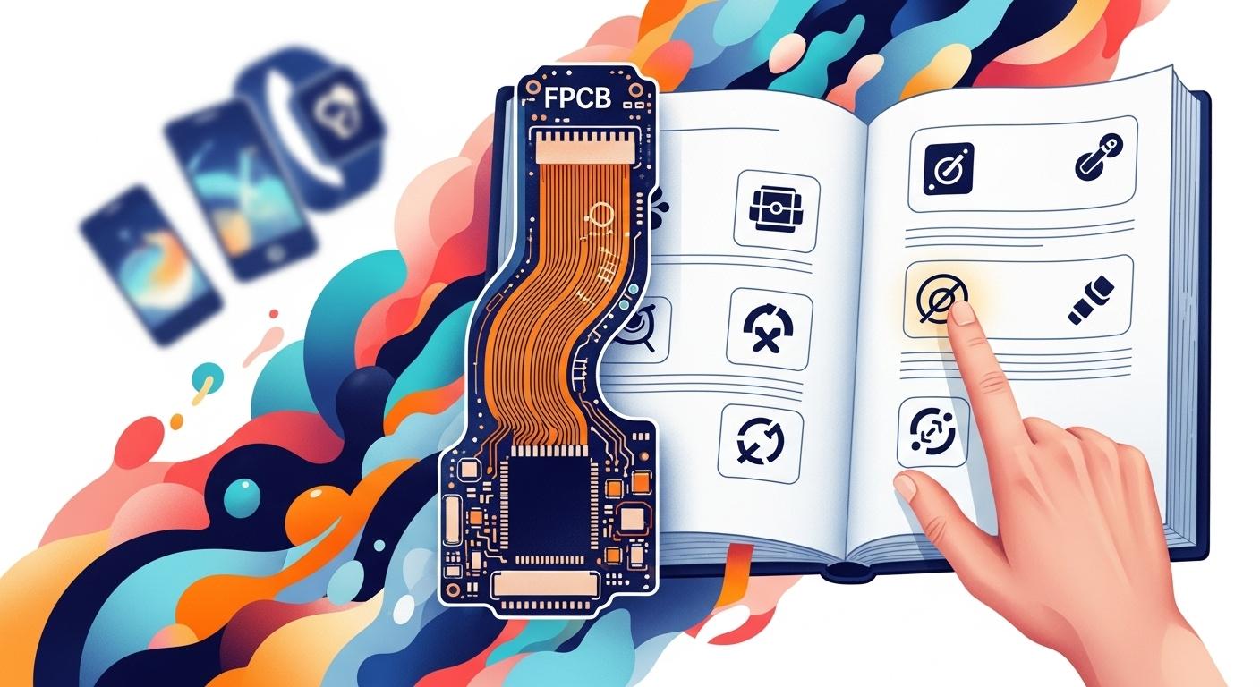
When you start learning about flexible printed circuit boards, knowing the right fpcb information and pcb terms glossary helps you avoid common mistakes. You will use printed circuit board terminology every time you design a circuit board, read a datasheet, or talk with a manufacturer. Many beginners face issues like unclear communication, trouble with design software, or errors in circuit board specifications.
- Miscommunication with manufacturers
- Difficulties reading printed circuit board technical specifications
- Challenges using design software
- Errors in board details that cause manufacturing issues
FPCB and rigid PCB serve different roles. Flexible printed circuit boards bend and fit into tight spaces, while rigid circuit boards stay flat and stiff. Use this pcb terms glossary to make circuit board projects easier and understand every board and circuit detail.
Key Takeaways
- Understanding FPCB terminology is crucial for effective communication with manufacturers and avoiding design errors.
- Flexible printed circuit boards (FPCBs) are ideal for compact designs, allowing circuits to bend and fit into tight spaces.
- Choosing the right materials and connectors is essential for ensuring the quality and performance of your circuit board.
- Common mistakes include neglecting bend radius checks and insufficient documentation; always double-check your design.
- Regularly review the glossary of terms to enhance your circuit board skills and improve project outcomes.
FPCB Information Basics
What is a Flexible Printed Circuit Board?
You use a flexible printed circuit board when you need a circuit that can bend or twist. This type of board uses flexible materials, which let you fit the circuit into small or oddly shaped spaces. You often see flex pcbs in devices where space is tight or where the circuit must move. The flexible design helps you connect components in ways that rigid boards cannot. Each component sits on the board, and the circuit connects them to make the device work. Flex pcbs make it easier to create lightweight and compact products.
FPCB vs PCB
You might wonder how a flexible printed circuit board differs from a rigid one. The main difference comes from the materials and how you use them in your design. Here is a table to help you compare:
| Feature | Flexible PCBs | Rigid PCBs |
|---|---|---|
| Flexibility | Designed to be flexible and bendable | Non-flexible, maintains shape |
| Material | Made from flexible substrates | Made from rigid insulating substrates |
| Applications | Ideal for space-constrained designs | Provides stable support for components |
| Weight | Lightweight and durable | Generally heavier due to materials |
| Manufacturing Cost | More expensive to manufacture | Typically less expensive |
You use a flexible printed circuit board when you need to bend the circuit or fit it into a small device. Rigid flex pcbs combine both types, giving you the benefits of flexibility and strong support for components.
Applications of FPCBs
You find flexible printed circuit boards in many modern devices. Here are some common uses:
- Smartphones
- Tablets
- Laptops
- Wearable devices
Flex pcbs also appear in electric vehicles and aerospace systems. The flexible design lets you fit the circuit board into tight spaces and adapt to movement. This reduces the weight of the device and helps you use energy more efficiently. You can connect more components in a smaller area, which makes your design more powerful. Rigid flex pcbs give you even more options by combining flexible and rigid sections for complex circuit layouts.
Glossary of FPCB Terminology
Understanding essential circuit board terminology helps you communicate with manufacturers and design better products. This glossary covers the most important terms you will encounter in flexible printed circuit board projects. You can use these definitions to improve your circuit board assembly and avoid mistakes during circuit board manufacturing.
Flex Circuit
A flex circuit is a printed circuit made of thin, flexible material. You use flex circuits when you need a circuit board that bends or twists to fit into small spaces. These printed circuits appear in smart home appliances, wearable devices, and other compact electronics. Flex circuits allow you to create innovative designs that improve both the look and function of modern technology. You will see flex circuits in many pcb projects because they make your circuit board design more versatile.
Tip: When you work with flex circuits, always check the material’s bend radius to avoid damaging the printed circuit.
Adhesives
Adhesives hold the layers of your printed circuit together. You use adhesives to bond the flexible base material to other layers, such as copper traces or stiffeners. Good adhesives keep your circuit board strong and prevent layers from peeling apart. You need to choose the right adhesive for your pcb to ensure quality control and long-lasting performance. Adhesives play a key role in circuit board manufacturing, especially for flexible designs.
Connectors
Connectors join different parts of your circuit board. You use connectors to link boards, wires, and components so signals and power can move between them. Connectors also keep your printed circuit stable and secure. Here is a table showing common connector functions and types:
| Function/Type | Description |
|---|---|
| Linking circuit boards | Connectors link different circuit boards together for integrated functionality. |
| Power and signal transmission | They facilitate the transfer of power and signals between components. |
| Mechanical stability | Connectors ensure that the physical connections remain stable and secure. |
| Board-to-board | Connectors that connect two circuit boards directly. |
| Wire-to-board | Connectors that connect wires to a circuit board. |
| Wire-to-wire | Connectors that link two wires together. |
| Card edge | Connectors that allow a circuit board to connect to another board. |
| Pin headers | Connectors with pins that allow for easy connection to other components. |
| Backplane | Connectors that connect multiple circuit boards in a system. |
| Surface-mount | Connectors designed for surface mounting on pcbs. |
| Specialized connectors | Includes formats like USB, coaxial, and circular connectors for specific uses. |
You need to select connectors that match your circuit board design and the components you use. The right connector improves the reliability of your pcb and makes your circuit board assembly easier.
Base Material
The base material forms the foundation of your printed circuit. You use flexible base materials, such as polyimide or polyester, for flex pcbs. The base material supports the copper traces and other layers. You must choose a base material that fits your circuit board’s needs, such as flexibility, heat resistance, and durability. The base material affects the overall quality and performance of your pcb.
Trace
A trace is a thin line of copper on your printed circuit. You use traces to connect components and carry signals or power across the board. Traces form the pathways that link each part of your circuit. You need to design traces carefully to avoid short circuits and ensure your pcb works as intended. Traces are a key part of circuit board terminology and play a major role in circuit design.
Solder Mask
The solder mask is a protective layer on your printed circuit. You use solder masks to cover the traces and prevent accidental solder bridges during assembly. Solder masks also protect the copper from moisture and dust. You need to apply the solder mask correctly to maintain the quality of your pcb and avoid problems during circuit board manufacturing.
Stiffener
A stiffener adds support to flexible areas of your printed circuit. You use stiffeners to strengthen parts of the board that need extra rigidity, such as connector locations or mounting points. Stiffeners help your pcb keep its shape and prevent damage during use. You must place stiffeners in the right spots to balance flexibility and strength in your circuit board design.
Via
A via is a small hole in your printed circuit that connects traces on different layers. You use vias to route signals between layers and link components across the board. Vias make your pcb more complex and allow for advanced circuit designs. You need to plan via placement carefully to avoid signal loss and ensure reliable connections.
Lamination
Lamination is the process of bonding layers together in your printed circuit. You use lamination to combine the base material, copper traces, adhesives, and other layers into a single board. Lamination improves the strength and durability of your pcb. You must control the lamination process to maintain quality control and prevent defects in your circuit board.
Note: You can use this glossary to check circuit board terminology during your next project. Understanding these terms helps you avoid mistakes and improve your circuit board manufacturing results.
Printed Circuit Board Design Tips
Material Selection
Choosing the right materials for your printed circuit board is one of the most important steps in pcb design. You need to think about how the circuit board will bend, how much weight it can handle, and how it will perform during assembly. Always check if your fabricator has the technical capabilities to handle complex designs. Quality control matters, so inspect all incoming materials and use advanced equipment for pcb testing & inspection. Make sure the materials you select meet the unique needs of flexible printed circuit boards. The table below shows key factors to consider:
| Factor | Description |
|---|---|
| Technical Capabilities | Choose a fabricator with advanced equipment and expertise for complex needs. |
| Quality Control | Inspect incoming materials and conduct in-process checks with advanced equipment. |
| Specific Requirements | Ensure the materials meet the unique demands of flexible PCBs, such as weight and flexibility. |
You can use a pcb stack-up guide to help you select the right layers for your multi-layer pcb. This guide helps you understand how each layer affects the performance of your circuit.
Design Constraints
When you start a pcb design, you will face several design constraints. These can affect how your printed circuit board works and how easy it is to assemble. You must pay attention to component spacing, signal routing, and power distribution. The table below lists common constraints and solutions:
| Design Constraint | Solution |
|---|---|
| Inadequate Component Spacing | Follow recommended clearance guidelines and consider thermal management requirements. |
| Improper Signal Routing | Use appropriate trace widths, maintain proper signal return paths, and minimize crosstalk. |
| Neglecting Power Distribution | Design a robust power distribution network with sufficient copper thickness and proper placement of bypass capacitors. |
| Overlooking Manufacturing Constraints | Familiarize with manufacturer’s capabilities and apply their design rules to avoid production delays. |
| Insufficient Documentation | Create comprehensive design documentation, including BOM, assembly drawings, and fabrication notes. |
You should always review your pcb stack-up guide and check your design against the manufacturer’s rules. This helps you avoid problems during pcb assembly and testing.
Common Mistakes
Many beginners make similar mistakes when working on a printed circuit board. You might forget to check the bend radius for flexible areas or skip important steps in pcb testing & inspection. Some people use the wrong materials or ignore the pcb stack-up guide. Others do not provide enough documentation for assembly, which can lead to errors during the build. You should always double-check your circuit board design, review your assembly drawings, and use the glossary to understand every term. This will help you avoid costly errors and improve your pcb assembly results.
Tip: Keep your glossary handy during every stage of your circuit board project. It will help you communicate better and catch mistakes before they become problems.
You improve every circuit board project when you master printed circuit board terminology. Clear terminology helps you communicate with manufacturers and avoid errors in circuit board design. The table below shows how understanding terminology leads to better results for your printed circuit board and circuit board assembly.
| Benefit of Mastering FPCB Terminology | Description |
|---|---|
| Effective Communication | You explain circuit board requirements clearly to manufacturers. |
| Reduced Errors | You prevent mistakes during printed circuit board production. |
| Improved Evaluation | You check circuit board specifications and quality with confidence. |
| Compliance with Standards | You follow printed circuit board standards for successful projects. |
Keep using the glossary as you work on each board and printed circuit board design. You build stronger circuit board skills when you review terminology often. For more learning, try these steps:
- Take online courses about printed circuit board and circuit board design.
- Use PCB design software to practice terminology and board layout.
- Work on real circuit board projects to apply terminology.
- Join online communities to discuss printed circuit board topics.
- Attend workshops for hands-on circuit board experience.
Tip: You boost your printed circuit board knowledge when you use the glossary and keep learning about terminology.
.png)
.png)
.png)
.png)

.png)

