


 2025-10-21
 BEST
BEST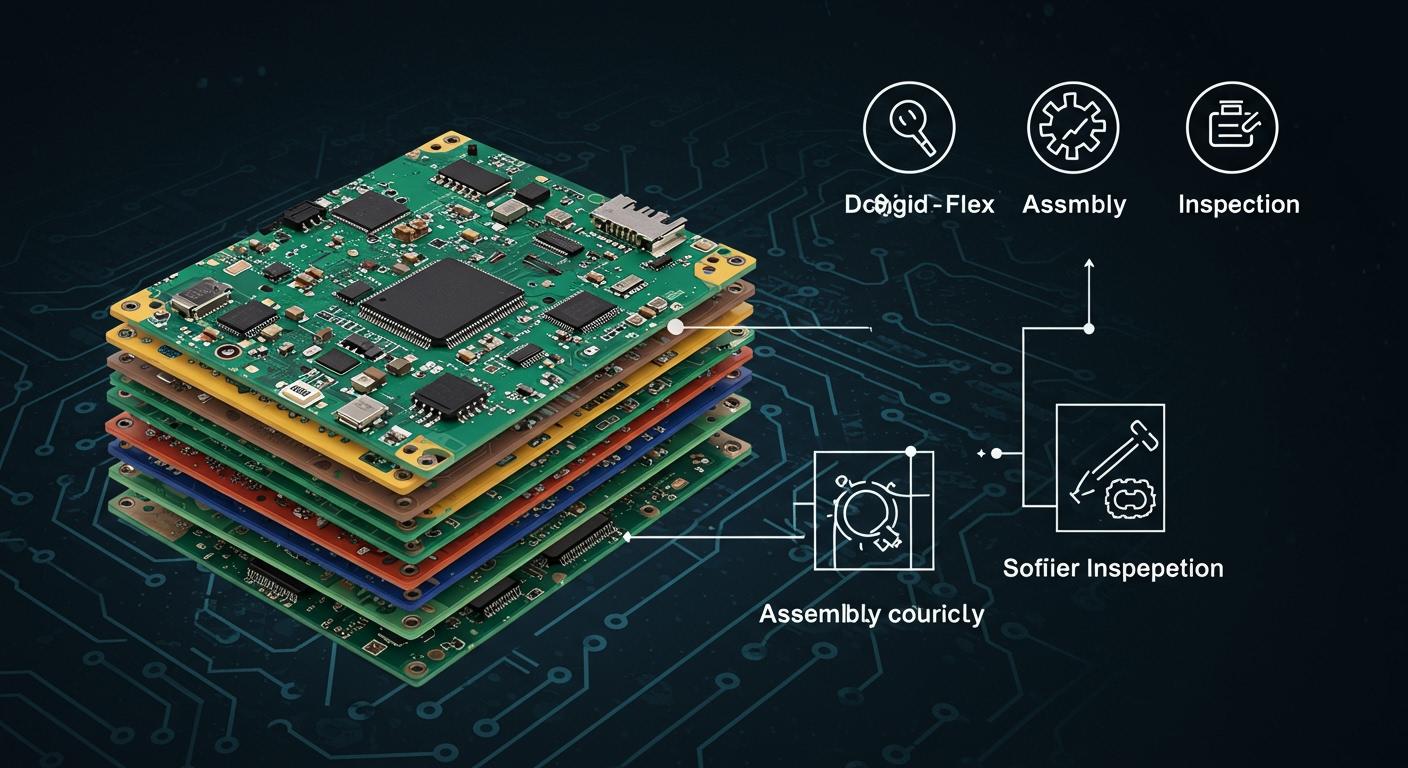
You need to approach a 6 layer rigid flex stackup with precision and attention to detail. Careful planning ensures you select materials with the right electrical and mechanical properties. Manufacturability becomes critical, as you must address challenges such as increased cost, tight registration tolerances, and complex panelisation. Quality assurance requires rigorous inspection and testing, since rework after fabrication proves difficult.
Common challenges include:
- Increased cost with each added layer
- Handling thin multilayer panels
- Tight alignment tolerances for dense vias
- High aspect ratio holes
- Strict fabrication limits
- Rigorous testing requirements
- Difficulties in rework
By focusing on the right materials, optimal layer arrangement, and precise fabrication, you avoid common pitfalls and achieve reliable results.
Key Takeaways
- Choose materials wisely. Select polyimide films for flexibility and FR-4 laminates for rigidity. Ensure adhesives and copper foils meet your design needs.
- Plan your stackup carefully. Arrange layers to enhance signal integrity and reduce stress. Use staggered routing and separate analogue from digital signals.
- Maintain strict quality control. Inspect and test at every stage to catch defects early. This ensures your stackup meets performance and reliability standards.
- Document everything. Provide clear guidelines for materials and processes. Good documentation helps avoid errors during fabrication.
- Collaborate with your manufacturer. Discuss material compatibility and fabrication challenges to simplify the design process and reduce costs.
6 Layer Rigid Flex Stackup Planning
Material Selection
You must select materials that meet both electrical and mechanical requirements for your 6 layer rigid flex stackup. Polyimide films offer flexibility and durability in the flex zones, while FR-4 laminates provide rigidity and stability in the stiff sections. Adhesives must withstand repeated bending and thermal cycles. Copper foils should have the right thickness for current carrying capacity and signal integrity. Always consult your manufacturer to ensure material compatibility and availability.
Layer Arrangement
The way you arrange layers in a 6 layer rigid flex stackup directly impacts signal integrity and reliability. You need to consider controlled impedance, routing challenges, and mechanical stress. Proper layer arrangement allows signals to travel with minimal loss and reduces the risk of crosstalk. You should use curved traces and staggered routing to minimise stress on the circuits. When moving from a 4-layer to a 6-layer design, you gain extra planes for power and ground, which improves noise immunity and supports higher routing density.
Tip: Plan your stackup with these factors in mind:
- Performance: Match materials and impedance to your circuit speed and environment.
- Cost: Collaborate with your manufacturer to balance performance and budget.
- Density: Anticipate routing needs to avoid costly redesigns.
- Circuitry: Separate analogue and digital signals and use stripline configurations for sensitive traces.
Rigid and Flex Zones
You must clearly define which areas of your PCB will be rigid and which will be flexible. Rigid zones support components and connectors, while flex zones allow the board to bend and fit into tight spaces. Assign each layer a specific function, such as signal, power, or ground, and ensure that only the required layers extend into the flex regions. This approach reduces stress and prevents unnecessary thickness in the flexible areas.
Stackup Structure
A well-structured 6 layer rigid flex stackup ensures both performance and manufacturability. Below is a typical architecture for such a stackup:
| Layer | Description | Rigid Zone | Flex Zone |
|---|---|---|---|
| 1 | Signal | ✔ | ✔ |
| 2 | Ground Plane | ✔ | ✔ |
| 3 | Signal | ✔ | ✔ |
| 4 | Signal | ✔ | ✔ |
| 5 | Power Plane | ✔ | ✔ |
| 6 | Signal | ✔ | ✔ |
You can adjust which layers extend into the flex area based on your design needs. Always keep the flex region as thin as possible for better bendability and reliability.
DFM and Documentation
Manufacturability
You must address manufacturability early in your design process. A 6 layer rigid flex stackup introduces unique challenges that require careful planning. The table below highlights the most common manufacturing challenges you may encounter:
| Challenge | Description |
|---|---|
| Complexity | More complex designs require advanced expertise and tools. |
| Cost | Higher material and manufacturing costs compared to rigid PCBs. |
| Manufacturing Equipment | Specialised equipment is often required, adding to production costs. |
| Structural Integrity | Maintaining integrity over the product lifecycle can be challenging. |
You can reduce risks by collaborating closely with your manufacturer. Choose stackup structures that simplify fabrication and avoid unnecessary complexity.
Impedance and Signal Integrity
You must control impedance to maintain signal integrity, especially as layer count increases. Use controlled impedance traces for high-speed signals. Place ground and power planes strategically to minimise noise and crosstalk. Keep trace widths and spacing consistent. Discuss impedance requirements with your manufacturer to ensure the finished board meets your performance targets.
Bend Radius
You must respect bend radius guidelines to ensure mechanical reliability. Follow these best practices:
- Keep the bend radius at least 10 times the thickness of the flexible material.
- Use flexible materials less than 0.2mm thick for optimal performance.
- Avoid tight bends, as they increase stress at material junctions and raise the risk of delamination.
- Repeated flexing with a small bend radius can cause stress fractures in copper tracks.
- The copper-to-film bond is critical; tighter bends increase boundary stresses and may compromise reliability.
Tip: Always design with a generous bend radius to extend the lifespan of your 6 layer rigid flex stackup.
Documentation
Comprehensive documentation is essential for flawless fabrication. You should provide clear guidelines for materials, stackup structure, and inspection criteria. Well-prepared documentation helps your manufacturer avoid errors and ensures each process step meets industry standards. By following IPC standards, you reduce the risk of defects and improve the reliability of your finished product.
Fabrication and Quality Assurance

Lamination
You must approach lamination with precision to achieve a flawless 6 layer rigid flex stackup. The process bonds multiple layers under heat and pressure. Common defects can compromise your board’s reliability. Watch for these issues:
- Delamination: Layers separate due to poor bonding, causing electrical failures.
- Voids: Air pockets form within layers, weakening the structure and disrupting signals.
- Warpage: The board bends or twists, making assembly difficult.
- Registration issues: Layers misalign, leading to misplaced vias and traces.
You can reduce these risks by controlling temperature, pressure, and humidity during lamination. Always inspect each panel before moving to the next step.
Drilling and Plating
Drilling and plating create reliable electrical connections between layers. You must follow best practices to ensure via reliability:
- Maintain proper aspect ratios. For through-hole drills, keep a 1:10 ratio. For HDI drills, use a 1:0.75 ratio.
- Choose the right via types. Select blind, buried, or microvias based on your design. Avoid too many vias in fine-pitch areas.
- Ensure effective signal return paths. Use ground or power planes to support signal integrity.
Careful drilling and plating prevent defects and improve the long-term performance of your stackup.
Etching and Stripping
Etching removes unwanted copper, while stripping clears away photoresist. You must monitor these steps closely. Uneven etching can cause open circuits or shorts. Precise stripping ensures clean traces and pads. Always check for residue or undercutting before moving forward.
Inspection and Testing
Inspection and testing confirm the quality of your finished board. Use automated optical inspection (AOI) to spot defects early. Electrical testing checks for continuity and isolation. You should also perform bend tests in the flex zones. These steps ensure your 6 layer rigid flex stackup meets all performance and reliability standards.
Tip: Early detection of defects saves time and cost. Never skip inspection at any stage.
You achieve a flawless 6 layer rigid flex stackup by following three essential steps:
- Select the right materials for both rigid and flex zones.
- Plan your stackup with precision and clear documentation.
- Apply strict quality control during fabrication.
Remember: Careful planning and attention to detail set your designs apart. Consistent application of these steps ensures reliable, high-quality PCBs every time.
.png)
.png)
.png)
.png)

.png)

